ZHCSIL6E June 2017 – March 2019 66AK2G12
PRODUCTION DATA.
- 1器件概述
- 2修订历史记录
- 3Device Comparison
-
4Terminal Configuration and Functions
- 4.1 Pin Diagram
- 4.2 Pin Attributes
- 4.3 Signal Descriptions
- 4.4 Pin Multiplexing
- 4.5 Connections for Unused Pins
-
5Specifications
- 5.1 Absolute Maximum Ratings
- 5.2 ESD Ratings
- 5.3 Power-On-Hour (POH) Limits
- 5.4 Recommended Operating Conditions
- 5.5 Operating Performance Points
- 5.6 Power Consumption Summary
- 5.7
Electrical Characteristics
- Table 5-2 DDR3L SSTL DC Electrical Characteristics
- Table 5-3 I2C OPEN DRAIN DC Electrical Characteristics
- Table 5-4 Oscillators DC Electrical Characteristics
- Table 5-5 LVDS Input Buffer DC Electrical Characteristics
- Table 5-6 LVDS Output Buffer DC Electrical Characteristics
- Table 5-7 MLB LVDS Buffers DC Electrical Characteristics
- Table 5-8 PORn DC Electrical Characteristics
- Table 5-9 1.8-Volt I/O LVCMOS DC Electrical Characteristics
- Table 5-10 3.3-Volt I/O LVCMOS DC Electrical Characteristics
- 5.7.1 USB0_PHY and USB1_PHY DC Electrical Characteristics
- 5.7.2 PCIe SERDES DC Electrical Characteristics
- 5.8 Thermal Resistance Characteristics for ABY Package
- 5.9
Timing and Switching Characteristics
- 5.9.1 Power Supply Sequencing
- 5.9.2 Reset Timing
- 5.9.3
Clock Specifications
- 5.9.3.1 Input Clocks / Oscillators
- 5.9.3.2 Optional LVDS Clock Inputs Not Used
- 5.9.3.3 Optional Audio Oscillator (AUDOSC) with External Crystal Circuit
- 5.9.3.4 Optional Audio Oscillator (AUDOSC) with External LVCMOS Clock Source
- 5.9.3.5 Optional Audio Oscillator (AUDOSC) Not Used
- 5.9.3.6 Optional USB PHY Reference Clock
- 5.9.3.7 PCIe Reference Clock
- 5.9.3.8 Output Clocks
- 5.9.3.9 PLLs
- 5.9.3.10 Recommended Clock and Control Signal Transition Behavior
- 5.9.4
Peripherals
- 5.9.4.1 DCAN
- 5.9.4.2 DSS
- 5.9.4.3 DDR EMIF
- 5.9.4.4
EMAC
- 5.9.4.4.1 EMAC MDIO Interface Timings
- 5.9.4.4.2
EMAC MII Timings
- Table 5-28 Timing Requirements for MII_RXCLK—MII Operation
- Table 5-29 Timing Requirements for MII_TXCLK—MII Operation
- Table 5-30 Timing Requirements for EMAC MII Receive 10 Mbps and 100 Mbps
- Table 5-31 Switching Characteristics Over Recommended Operating Conditions for EMAC MII Transmit 10 Mbps and 100 Mbps
- 5.9.4.4.3
EMAC RMII Timings
- Table 5-32 Timing Requirements for EMAC RMII_REFCLK—RMII Operation
- Table 5-33 Timing Requirements for EMAC RMII Receive
- Table 5-34 Switching Characteristics Over Recommended Operating Conditions for EMAC RMII_REFCLK —RMII Operation
- Table 5-35 Switching Characteristics Over Recommended Operating Conditions for EMAC RMII Transmit 10 Mbps and 100 Mbps
- 5.9.4.4.4
EMAC RGMII Timings
- Table 5-36 Timing Requirements for RGMII_RXC—RGMII Operation
- Table 5-37 Timing Requirements for EMAC RGMII Input Receive for 10 Mbps, 100 Mbps, and 1000 Mbps
- Table 5-38 Switching Characteristics Over Recommended Operating Conditions for Transmit - RGMII operation for 10 Mbps, 100 Mbps, and 1000 Mbps
- Table 5-39 Switching Characteristics Over Recommended Operating Conditions for EMAC RGMII Transmit - RGMII_TXD[3:0], and RGMII_TXCTL - RGMII Mode
- Table 5-40 Switching Characteristics Over Recommended Operating Conditions for EMAC RGMII Transmit - RGMII_TXD[3:0], and RGMII_TXCTL - RGMII ID Mode
- 5.9.4.5 GPMC
- 5.9.4.6 I2C
- 5.9.4.7 McASP
- 5.9.4.8 McBSP
- 5.9.4.9 MLB
- 5.9.4.10
MMC/SD
- Table 5-60 MMC Timing Conditions
- Table 5-61 Timing Requirements for MMC0_CMD and MMC0_DATn
- Table 5-62 Timing Requirements for MMC1_CMD and MMC1_DATn when operating in SDR mode
- Table 5-63 Timing Requirements for MMC1_CMD and MMC1_DATn when operating in DDR mode
- Table 5-64 Switching Characteristics for MMCi_CLK
- Table 5-65 Switching Characteristics for MMC0_CMD and MMC0_DATn—HSPE=0
- Table 5-66 Switching Characteristics for MMC1_CMD and MMC1_DATn—HSPE=0 when operating in SDR mode
- Table 5-67 Switching Characteristics for MMC1_CMD and MMC1_DATn—HSPE=0 when operating in DDR mode
- 5.9.4.11 PCIESS
- 5.9.4.12
PRU-ICSS
- 5.9.4.12.1 Programmable Real-Time Unit (PRU-ICSS PRU)
- 5.9.4.12.2 PRU-ICSS EtherCAT (PRU-ICSS ECAT)
- 5.9.4.12.3 PRU-ICSS MII_RT and Switch
- 5.9.4.12.4 PRU-ICSS Universal Asynchronous Receiver Transmitter (PRU-ICSS UART)
- 5.9.4.12.5 PRU-ICSS PRU Sigma Delta and EnDAT Modes
- 5.9.4.13 QSPI
- 5.9.4.14 SPI
- 5.9.4.15 Timers
- 5.9.4.16 UART
- 5.9.4.17 USB
- 5.9.5 Emulation and Debug Subsystem
- 6Detailed Description
-
7Applications, Implementation, and Layout
- 7.1
DDR3L Board Design and Layout Guidelines
- 7.1.1 DDR3L General Board Layout Guidelines
- 7.1.2
DDR3L Board Design and Layout Guidelines
- 7.1.2.1 Board Designs
- 7.1.2.2 DDR3L Device Combinations
- 7.1.2.3 DDR3L Interface Schematic
- 7.1.2.4 Compatible JEDEC DDR3L Devices
- 7.1.2.5 PCB Stackup
- 7.1.2.6 Placement
- 7.1.2.7 DDR3L Keepout Region
- 7.1.2.8 Bulk Bypass Capacitors
- 7.1.2.9 High-Speed Bypass Capacitors
- 7.1.2.10 Net Classes
- 7.1.2.11 DDR3L Signal Termination
- 7.1.2.12 VREF_DDR Routing
- 7.1.2.13 VTT
- 7.1.2.14 CK and ADDR_CTRL Topologies and Routing Definition
- 7.1.2.15 Data Topologies and Routing Definition
- 7.1.2.16 Routing Specification
- 7.2 High Speed Differential Signal Routing Guidance
- 7.3 Power Distribution Network (PDN) Implementation Guidance
- 7.4 Single-Ended Interfaces
- 7.5 Clock Routing Guidelines
- 7.1
DDR3L Board Design and Layout Guidelines
- 8Device and Documentation Support
- 9Mechanical Packaging and Orderable Information
5.1 Absolute Maximum Ratings
over operating junction temperature range (unless otherwise noted)(1)(2)| PARAMETERS | MIN | MAX | UNIT | ||
|---|---|---|---|---|---|
| VSUPPLY (steady-state) | Supply steady state voltage ranges | CVDD | -0.3 | 1.3 | V |
| CVDD1 | -0.3 | 1.3 | V | ||
| VPP2(5) | -0.3 | 1.98 | V | ||
| AVDDA_DDRPLL | -0.3 | 1.98 | V | ||
| AVDDA_DSSPLL | -0.3 | 1.98 | V | ||
| AVDDA_MAINPLL | -0.3 | 1.98 | V | ||
| AVDDA_NSSPLL | -0.3 | 1.98 | V | ||
| AVDDA_UARTPLL | -0.3 | 1.98 | V | ||
| AVDDA_ICSSPLL | -0.3 | 1.98 | V | ||
| AVDDA_ARMPLL | -0.3 | 1.98 | V | ||
| DVDD_DDR | -0.3 | 1.98 | V | ||
| DVDD_DDRDLL | -0.3 | 2.45 | V | ||
| VDDAHV | -0.3 | 2.45 | V | ||
| DVDD18 | -0.3 | 2.45 | V | ||
| DVDD33 | -0.3 | 3.63 | V | ||
| DVDD33_USB | -0.3 | 3.63 | V | ||
| VIO (steady-state) | Non-fail-safe IO steady-state voltage ranges(3)(6) | All IOs which are not fail-safe | -0.3 | IO supply voltage + 0.3 | V |
| DDR3_VREFSSTL | 0.49 × DVDD_DDR | 0.51 × DVDD_DDR | V | ||
| Fail-safe IO steady-state voltage ranges(7) | USB0_VBUS | 0 | 5.25 | V | |
| USB1_VBUS | 0 | 5.25 | V | ||
| SR | Maximum slew rate | All supplies except VPP2 | 1 × 10⁵ | V/s | |
| VPP2 | 0.6 × 10⁵ | V/s | |||
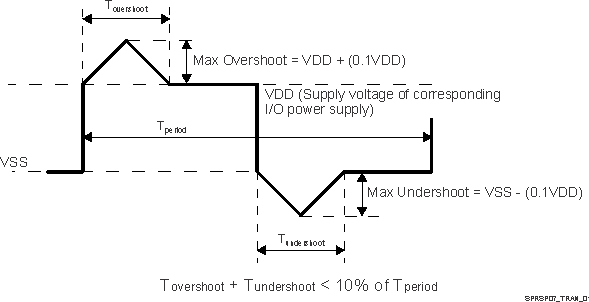
| VIO (transient overshoot and undershoot) | IO transient voltage ranges (transient overshoot and undershoot)(4) | I2C IOs(8) | 10% overshoot / undershoot for 10% of signal duty cycle
(see Figure 5-1) |
V | |
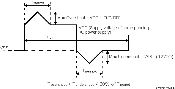
| All other IOs | 20% overshoot / undershoot for 20% of signal duty cycle
(see Figure 5-2) |
V | |||
| TSTG | Storage temperature after soldered onto PC board | -65 | 150 | °C | |
- Stresses beyond those listed under Absolute Maximum Ratings may cause permanent damage to the device. These are stress ratings only, and functional operation of the device at these or any other conditions beyond those indicated under Section 5.4, Recommended Operating Conditions is not implied. Exposure to absolute-maximum-rated conditions for extended periods may affect device reliability.
- All voltage values are with respect to VSS, unless otherwise noted.
- Refer to Table 4-1, Pin Attributes to determine which power supply is associated with an IO.
- Overshoot/Undershoot percentage relative to IO operating values - for example the maximum overshoot value for a standard LVCMOS IO operating at 1.8 V is DVDD18 + (0.20 × DVDD18) and maximum undershoot value would be VSS - (0.20 × DVDD18).
- The VPP2 power supply pin is only valid for high-security (66AK2G1xS) devices. The VPP2 power source shall only be enabled while programming the customer OTP eFuse array and shall be disabled during power-up sequence, normal operation, and power-down sequence. When disabled, the power source shall not source current to, or sink current from the VPP2 terminal. This power supply pin is reserved for general purpose (66AK2G1x) devices and shall not be connected to any signal, test point, or printed circuit board trace when using 66AK2G1x devices.
- This parameter applies to all IO terminals which are not fail-safe and the requirement applies to all values of IO supply voltage. For example, if the voltage applied to a specific IO supply is 0 volts the valid input voltage range for any IO powered by that supply will be –0.3 V to +0.3 V. Apply special attention anytime peripheral devices are not powered from the same power sources used to power the respective IO supply. It is important the attached peripheral never sources a voltage outside the valid input voltage range, including power supply ramp-up and ramp-down sequences.
- This parameter is associated with a fail-safe IO and does not have a dependence on any IO supply voltage.
- Designing a system that is able to meet the I2C overshoot/undershoot limit defined by this parameter should not be an issue since the I2C specification defines a minimum rise/fall time which minimizes overshoots and undershoots. However, special design precautions may need to be taken if the I2C IOs are connected to other devices which are not compliant to the minimum rise/fall time parameters defined in the I2C specification.
 Figure 5-1 I2C I/O transient voltage ranges
  Figure 5-2 All other I/Os transient voltage ranges