ZHCSEA4C May 2015 – December 2020 ADS54J40
PRODUCTION DATA
- 1 特性
- 2 应用
- 3 说明
- 4 Revision History
- 5 ADS54J40 Comparison
- 6 Pin Configuration and Functions
- 7 Specifications
-
8 Detailed Description
- 8.1 Overview
- 8.2 Functional Block Diagram
- 8.3 Feature Description
- 8.4 Device Functional Modes
- 8.5
Register Maps
- 8.5.1 Example Register Writes
- 8.5.2
Register Descriptions
- 8.5.2.1 General Registers
- 8.5.2.2
Master Page (080h) Registers
- 8.5.2.2.1 Register 20h (address = 20h), Master Page (080h)
- 8.5.2.2.2 Register 21h (address = 21h), Master Page (080h)
- 8.5.2.2.3 Register 23h (address = 23h), Master Page (080h)
- 8.5.2.2.4 Register 24h (address = 24h), Master Page (080h)
- 8.5.2.2.5 Register 26h (address = 26h), Master Page (080h)
- 8.5.2.2.6 Register 4Fh (address = 4Fh), Master Page (080h)
- 8.5.2.2.7 Register 53h (address = 53h), Master Page (080h)
- 8.5.2.2.8 Register 54h (address = 54h), Master Page (080h)
- 8.5.2.2.9 Register 55h (address = 55h), Master Page (080h)
- 8.5.2.2.10 Register 59h (address = 59h), Master Page (080h)
- 8.5.2.3 ADC Page (0Fh) Register
- 8.5.2.4
Main Digital Page (6800h) Registers
- 8.5.2.4.1 Register 0h (address = 0h), Main Digital Page (6800h)
- 8.5.2.4.2 Register 40h (address = 40h), Main Digital Page (6800h)
- 8.5.2.4.3 Register 41h (address = 41h), Main Digital Page (6800h)
- 8.5.2.4.4 Register 42h (address = 42h), Main Digital Page (6800h)
- 8.5.2.4.5 Register 43h (address = 43h), Main Digital Page (6800h)
- 8.5.2.4.6 Register 44h (address = 44h), Main Digital Page (6800h)
- 8.5.2.4.7 Register 4Bh (address = 4Bh), Main Digital Page (6800h)
- 8.5.2.4.8 Register 4Dh (address = 4Dh), Main Digital Page (6800h)
- 8.5.2.4.9 Register 4Eh (address = 4Eh), Main Digital Page (6800h)
- 8.5.2.4.10 Register 52h (address = 52h), Main Digital Page (6800h)
- 8.5.2.4.11 Register 68h (address = 68h), Main Digital Page (6800h)
- 8.5.2.4.12 Register 72h (address = 72h), Main Digital Page (6800h)
- 8.5.2.4.13 Register ABh (address = ABh), Main Digital Page (6800h)
- 8.5.2.4.14 Register ADh (address = ADh), Main Digital Page (6800h)
- 8.5.2.4.15 Register F7h (address = F7h), Main Digital Page (6800h)
- 8.5.2.5
JESD Digital Page (6900h) Registers
- 8.5.2.5.1 Register 0h (address = 0h), JESD Digital Page (6900h)
- 8.5.2.5.2 Register 1h (address = 1h), JESD Digital Page (6900h)
- 8.5.2.5.3 Register 2h (address = 2h), JESD Digital Page (6900h)
- 8.5.2.5.4 Register 3h (address = 3h), JESD Digital Page (6900h)
- 8.5.2.5.5 Register 5h (address = 5h), JESD Digital Page (6900h)
- 8.5.2.5.6 Register 6h (address = 6h), JESD Digital Page (6900h)
- 8.5.2.5.7 Register 7h (address = 7h), JESD Digital Page (6900h)
- 8.5.2.5.8 Register 16h (address = 16h), JESD Digital Page (6900h)
- 8.5.2.5.9 Register 31h (address = 31h), JESD Digital Page (6900h)
- 8.5.2.5.10 Register 32h (address = 32h), JESD Digital Page (6900h)
- 8.5.2.6
JESD Analog Page (6A00h) Registers
- 8.5.2.6.1 Register 12h (address = 12h), JESD Analog Page (6A00h)
- 8.5.2.6.2 Registers 13h-15h (addresses = 13h-5h), JESD Analog Page (6A00h)
- 8.5.2.6.3 Register 16h (address = 16h), JESD Analog Page (6A00h)
- 8.5.2.6.4 Register 17h (address = 17h), JESD Analog Page (6A00h)
- 8.5.2.6.5 Register 1Ah (address = 1Ah), JESD Analog Page (6A00h)
- 8.5.2.6.6 Register 1Bh (address = 1Bh), JESD Analog Page (6A00h)
- 8.5.2.7
Offset Read Page (JESD BANK PAGE SEL = 6100h, JESD BANK PAGE SEL1
= 0000h) Registers
- 8.5.2.7.1 Register 068h (address = 068h), Offset Read Page
- 8.5.2.7.2 Register 069h (address = 069h), Offset Read Page
- 8.5.2.7.3 Registers 074h, 076h, 078h, 7Ah (address = 074h, 076h, 078h, 7Ah), Offset Read Page
- 8.5.2.7.4 Registers 075h, 077h, 079h, 7Bh (address = 075h, 077h, 079h, 7Bh), Offset Read Page
- 8.5.2.8 Offset Load Page (JESD BANK PAGE SEL= 6100h, JESD BANK PAGE SEL1 = 0500h) Registers
- 9 Application Information Disclaimer
- 10Power Supply Recommendations
- 11Layout
- 12Device and Documentation Support
9.1.6.2 Features
- IL mismatch correction has 2 components – Analog Correction component and Digital Correction component. The correction parameters are provided by the ‘IL Mismatch Parameters Estimator’ block shown in Fig 1.
- Tracking of IL mismatch parameters happens continuously in the background, based on incoming data (except under certain specific conditions listed in item 5).
- IL mismatch estimation uses Nyquist band information programmed by the user, for
proper estimation from the input signals. Note that for higher Nyquist signals,
the IL spurs are at Fin_alias + kFs/4 (k = 1,2,3) where Fin_alias is the aliased
input frequency between [-Fs/2,Fs/2]. This effectively gives the location of IL
spurs at the ADC output.
- Any change in Nyquist band should be succeeded by a “pulse reset”. A pulse reset signal resets the internal IL mismatch estimation and correction and the JESD link. However; all other registers written into the IL engine or the status of the rest of the system is unaffected by a pulse reset. The IL mismatch parameters would be reestimated for the new Nyquist band after a pulse reset
- In typical use cases, signals would be present
only within one Nyquist band. However, if there
are signals across multiple Nyquist bands (for eg
the desired bands in multiple Nyquist bands may
not alias after sampling enabling them to be
separated later), it is possible that IL
performance may be degraded. So it is advisable to
disable IL engine to get raw IL performance. The
typical raw IL performance is shown in Figure 9-10.
 Figure 9-10 Typical raw IL Performance.
 Typical raw IL Performance
- IL image performance starts to degrade gracefully for signal frequency
components > 0.9 x Fs/2, for 1st Nyquist signals, as digital correction cannot
accurately correct for signals very close to Nyquist band edge .
- For signals in higher Nyquist bands, the performance degrades gracefully for aliased frequency components <0.1Fs/2 or >0.9Fs/2
- IL correction accuracy will continue to be maintained unless any of the
following conditions are hit:
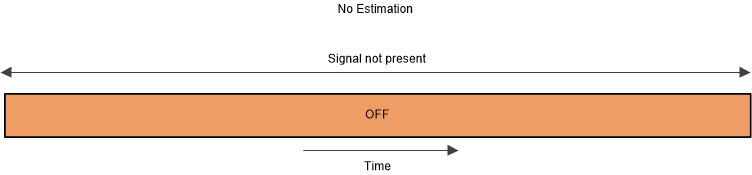
- Persistent Signal absence: The IL estimator works
on the input signals to estimate and track IL
mismatch parameters over time. So if no input
signal is present, then IL mismatch estimation is
not possible. See item 5f for further
details.
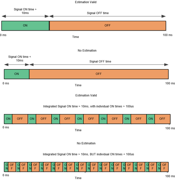
- Persistent very weak signal only: As IL estimator
works on input signals, it needs
reasonable-powered signals present for some
continuous period of time to get IL estimates
properly. The signal power in atleast one
frequency band of width Fs/256 has to be > -35
dBFs for proper IL estimation. Further such signal
needs to be present in chunks of atleast 100 µs
for an integrated ON period of at least 10 ms over
a total time of 100 ms for proper IL estimation.
See item 5f for further details.
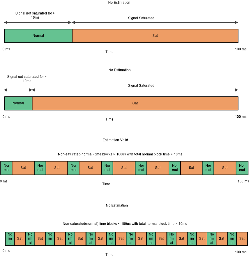
- Consistent Signal saturation: Whenever signal is
saturated, signal gets distorted and IL estimation
is no longer possible. IL estimation is possible
if signal amplitude is < -0.5 dBFs for more
than 100 µs in one chunk and such chunks make up
atleast 10 ms in a 100 ms window. See item 5f for
further details.
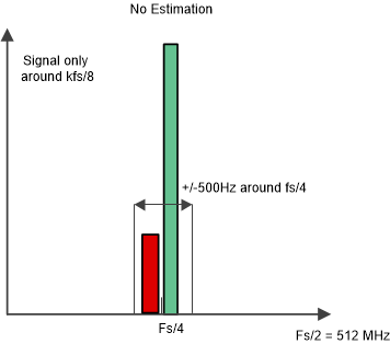
- Signal presence in a very small band only around
kfs/8: If input signal is present only within 5e-7
x Fs of kFs/8 (k = 0,1,2,3), then no IL estimation
is possible as the IL signal and IL image are not
separable. See item 5f for further details.
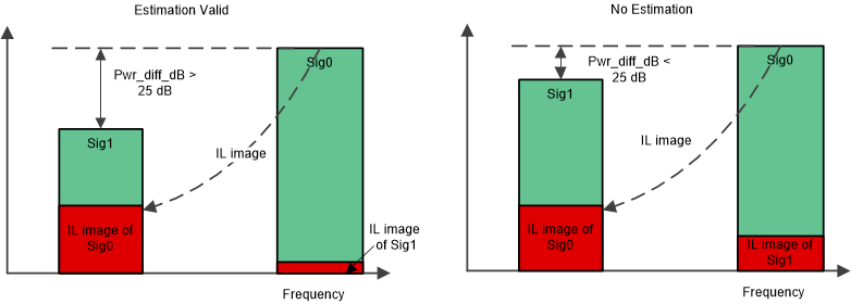
- Presence of high power signal component in the IL
image band: In some cases, the signal component
(such as Sig1) may be present in the IL image band
of other components of the signal (such as Sig0).
This signal component in IL image band (Sig1) acts
as an interferer for IL estimation of the first
component (Sig0). If the ratio of the power of the
signal component causing IL mismatch (power of
Sig0) to the power of the signal component in the
IL image band (power of Sig1) is less than 25 dB,
then IL estimation cannot be done for that signal
component (Sig0). See item 5f for further
details
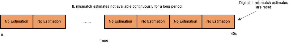
- In the normal course of operation, old IL
mismatch estimates are retained and used for
correction even if there are no current IL
mismatch estimates due to any of the conditions
listed in 5a – 5e. This enables good performance
when any of the conditions in 5a-5e are present
for a short duration. However if any of the
conditions that prevent estimation listed in 5a –
5e persist for a large time (>40s), then the
estimated digital IL mismatch parameters are reset
and the digital IL mismatch parameters are
re-estimated when the conditions for estimation
becomes favorable again.
- If the user knows apriori that such a condition will occur and would like the old IL correction to be retained, then a good option is to freeze the IL engine as in item 6. This freeze stops the IL engine and so the old IL estimates are not discarded.
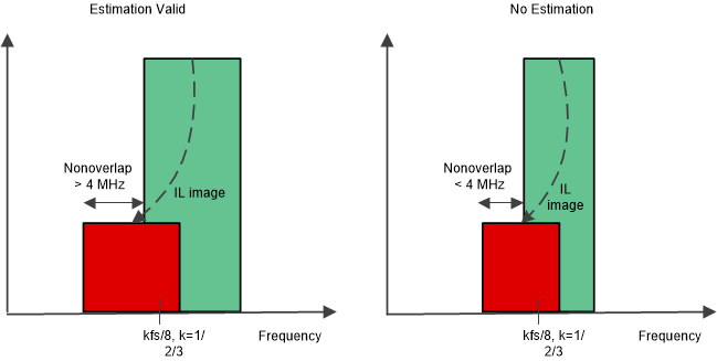
- Signal and IL image overlap: If signal component
is present around kfs/8 (k = 0,1,2,3), then the IL
image band will also overlap with the signal
making it difficult to estimate IL mismatch
parameters. Overlap of signal and IL image bands
around kfs/8 should be < Fs/256 MHz for 90% of
the time for proper IL estimation. Note that if
this condition cannot be ensured, then IL
performance will be degraded. If this condition is
violated in a known period, then the user can
freeze IL engine when this condition occurs as
described in section 6. Otherwise, user has to
switch to options in items 6 or 7 to avoid
performance degradation
- Persistent Signal absence: The IL estimator works
on the input signals to estimate and track IL
mismatch parameters over time. So if no input
signal is present, then IL mismatch estimation is
not possible. See item 5f for further
details.
- Freezing the IL Engine: If the user knows apriori that any of the conditions in
item 5f occurs and would like the old IL correction to be retained, then a good
option is to freeze the IL engine. Or, if the user knows that condition in 5g is
violated at a known time, then also freezing the IL engine is a good option.
Once IL engine is frozen, all past IL estimates/correction are retained and no
updates are done to the IL estimates. Once the conditions described above are no
longer present, then the IL engine can be unfrozen. The IL engine then starts
updating the estimates as though the entire period for which it was frozen did
not exist at all. Table 9-4 IL Freeze
SPI Address SPI Data Comments 0x4005 0x1 Enable per channel writes 0x4004 0x68 Page Select 0x4003 0x00 Page Select 0x4002 0x00 Page Select 0x4001 0x00 Page Select 0x604D 0x01 Validity for IL Freeze/Unfreeze for CHA 0x704D 0x01 Validity for IL Freeze/Unfreeze for CHB 0x6068 0x04 Freeze IL Engine for CHA 0x7068 0x04 Freeze IL Engine for CHB 0x4004 0x61 Page Select 0x4003 0x00 Page Select 0x4002 0x05 Page Select 0x4001 0x00 Page Select 0x6078 0x00 IL Engine Freeze Secondary Control for CHA 0x7078 0x00 IL Engine Freeze Secondary Control for CHB 0x4004 0x68 Page Select 0x4003 0x00 Page Select 0x4002 0x00 Page Select 0x4001 0x00 Page Select Table 9-5 IL UnfreezeSPI Address SPI Data Comments 0x4005 0x00 Enable per channel writes 0x4004 0x68 Page Select 0x4003 0x00 Page Select 0x4002 0x00 Page Select 0x4001 0x00 Page Select 0x604D 0x01 Validity for IL Freeze/Unfreeze for CHA 0x704D 0x01 Validity for IL Freeze/Unfreeze for CHB 0x6068 0x00 Unfreeze IL Engine for CHA 0x7068 0x00 Unfreeze IL Engine for CHB - In case the limitations in items 5 cannot be worked around in the user system
and the limitations are permanent (eg a system where the entire band from
[0,fs/2) is nearly fully occupied or signals present around kfs/8 with overlap
< Fs/256), then there are 2 options
- Power up/Temp based IL calibration - Do
calibration using a single tone (single tone
frequency in [0.77fs/2, 0.9 x fs/2], single tone
power in [-0.5, -25] dBFs), either one-time or
whenever temperature changes by more than a
desired threshold, and then freeze IL estimation
module. During calibration, the normal input
should be bypassed and the calibration signal
should be input to ADS54J40 for 100 ms for high
power signals (≥ - 3 dBFs) and 500 ms for lower
powered signals. Once the calibration time is
complete, IL estimation should be frozen and
normal signal may be input to ADS54J40. To
determine the temperature change for which
calibration needs to be done, the user can refer
to typical variation of IL spur with temperature,
under freeze conditions, as shown in Figure 9-11 .
 Figure 9-11 Flowchart for Powerup IL
Calibratuion
Figure 9-11 Flowchart for Powerup IL
Calibratuion Figure 9-12 Flow chart for intermittent IL
calibration
Figure 9-12 Flow chart for intermittent IL
calibration - Disable IL correction – IL performance would be limited to raw IL
performance as shown in figure in the data sheet. Note that the disable
IL correction sequence includes “pulse reset”. A pulse reset signal
resets the internal IL mismatch estimation and correction and the JESD
link. Therefore, in case IL correction disable is desired, it is
preferable to insert this sequence within the device bring up sequence,
just before the final pulse reset is issued.Table 9-6 IL Disable
SPI Address SPI Data Comments 0x4005 0x0 Enable single channel writes 0x4004 0x68 Selecting page 0x4003 0x00 Selecting page 0x4002 0x00 Selecting page 0x4001 0x00 Selecting page 0x604B 0x04 Validity for IL Correction Disable for CHA 0x704B 0x04 Validity for IL Correction Disable for CHB 0x6040 0x08 Disable IL Correction for CHA 0x7040 0x08 Disable IL Correction for CHB 0x6000 0x01 Pulse reset assert 0x6000 0x00 Pulse reset de-assert
- Power up/Temp based IL calibration - Do
calibration using a single tone (single tone
frequency in [0.77fs/2, 0.9 x fs/2], single tone
power in [-0.5, -25] dBFs), either one-time or
whenever temperature changes by more than a
desired threshold, and then freeze IL estimation
module. During calibration, the normal input
should be bypassed and the calibration signal
should be input to ADS54J40 for 100 ms for high
power signals (≥ - 3 dBFs) and 500 ms for lower
powered signals. Once the calibration time is
complete, IL estimation should be frozen and
normal signal may be input to ADS54J40. To
determine the temperature change for which
calibration needs to be done, the user can refer
to typical variation of IL spur with temperature,
under freeze conditions, as shown in Figure 9-11 .