ZHCSH90A January 2015 – December 2017 VSP5324-Q1
PRODUCTION DATA.
- 1 特性
- 2 应用
- 3 说明
- 4 修订历史记录
- 5 Pin Configuration and Functions
-
6 Specifications
- 6.1 Absolute Maximum Ratings
- 6.2 ESD Ratings
- 6.3 Recommended Operating Conditions
- 6.4 Thermal Information
- 6.5 Electrical Characteristics: Dynamic Performance
- 6.6 Electrical Characteristics: General
- 6.7 Electrical Characteristics: Digital
- 6.8 Timing Requirements
- 6.9 LVDS Timing at Different Sampling Frequencies (One-Lane Interface, 12x Serialization)
- 6.10 LVDS Timing at Different Sampling Frequencies (Two-Lane Interface, 6x Serialization)
- 6.11 Serial Interface Timing Requirements
- 6.12 Typical Characteristics
-
7 Detailed Description
- 7.1 Overview
- 7.2 Functional Block Diagrams
- 7.3 Feature Description
- 7.4 Device Functional Modes
- 7.5 Programming
- 7.6
Register Maps
- 7.6.1
Serial Registers
- 7.6.1.1 Register 00h (offset = 00h) [reset = 0]
- 7.6.1.2 Register 01h (offset = 01h) [reset = 0]
- 7.6.1.3 Register 02h (offset = 02h) [reset = 0]
- 7.6.1.4 Register 0Ah (offset = 0Ah) [reset = 0]
- 7.6.1.5 Register 0Fh (offset = 0Fh) [reset = 0]
- 7.6.1.6 Register 14h (offset = 14h) [reset = 0]
- 7.6.1.7 Register 1Ch (offset = 1Ch) [reset = 0]
- 7.6.1.8 Register 23h (offset = 23h) [reset = 0]
- 7.6.1.9 Register 24h (offset = 24h) [reset = 0]
- 7.6.1.10 Register 25h (offset = 25h) [reset = 0]
- 7.6.1.11 Register 26h (offset = 26h) [reset = 0]
- 7.6.1.12 Register 27h (offset = 27h) [reset = 0]
- 7.6.1.13 Register 28h (offset = 28h) [reset = 0]
- 7.6.1.14 Register 29h (offset = 29h) [reset = 0]
- 7.6.1.15 Register 2Ah (offset = 2Ah) [reset = 0]
- 7.6.1.16 Register 2Bh (offset = 2Bh) [reset = 0]
- 7.6.1.17 Register 2Eh (offset = 2Eh) [reset = 0]
- 7.6.1.18 Register 30h (offset = 30h) [reset = 0]
- 7.6.1.19 Register 33h (offset = 33h) [reset = 0]
- 7.6.1.20 Register 35h (offset = 35h) [reset = 0]
- 7.6.1.21 Register 38h (offset = 38h) [reset = 0x0000]
- 7.6.1.22 Register 42h (offset = 42h) [reset = 0]
- 7.6.1.23 Register 45h (offset = 45h) [reset = 0]
- 7.6.1.24 Register 46h (offset = 46h) [reset = 0]
- 7.6.1.25 Register 50h (offset = 50h) [reset = 0]
- 7.6.1.26 Register 51h (offset = 51h) [reset = 0]
- 7.6.1.27 Register 53h (offset = 53h) [reset = 0]
- 7.6.1.28 Register 54h (offset = ) [reset = 0]
- 7.6.1.29 Register 55h (offset = 55h) [reset = 0]
- 7.6.1.30 Register F0h (offset = F0h) [reset = 0]
- 7.6.1
Serial Registers
- 8 Application and Implementation
- 9 Power Supply Recommendations
- 10Layout
- 11器件和文档支持
- 12机械、封装和可订购信息
7.5.3 Serial Register Readout
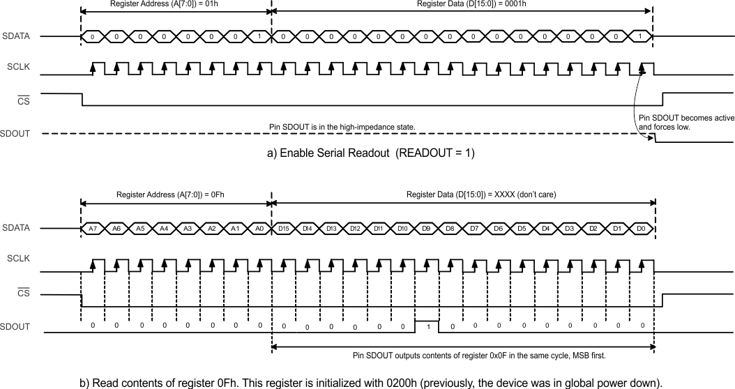
The device includes a mode where the contents of the internal registers can be readback on the SDOUT pin, as shown in Figure 49. This mode can useful as a diagnostic check to verify the serial interface communication between the external controller and ADC.
By default, after power-up and device reset, the SDOUT pin is high-impedance. When readout mode is enabled using the READOUT register bit, the SDOUT pin outputs the contents of the selected register serially in the following sequence:
- The READOUT register bit must be set to 1 in order for the device to enter readout mode. This setting disables any further writes into the internal registers, except for the register at address 01h. Note that the READOUT bit is also located in this register. The device can exit readout mode by writing the READOUT bit to 0. Only the register contents of address 01h are unable to be read in register readout mode.
- The read cycle is initiated by clocking the register address A[7:0] on the SDIN pin.
- The device serially outputs the contents (D[15:0]) of the selected register on the SDOUT pin.
- The external controller latches the contents at the SCLK rising edge.
- The READOUT register bit is set to 0 to exit serial readout mode, which enables all registers of the device to be written to. At this point, the SDOUT pin enters a high-impedance state.
 Figure 49. Serial Readout Timing
After reset, the device default states include the following:
- The device is in normal operation mode with 12x serialization enabled for all channels.
- Output interface is one-lane, 12x serialization with a 6x bit clock and a 1x frame clock frequency.
- Data format is LSB-first and offset binary.
- Serial readout is disabled.
- The PD pin is configured as a global power-down pin.
- Digital gain is set to 0 dB.