SPRUJ64 September 2022
- Abstract
- Trademarks
- 1Key Features
- 2AM64x SKEVM Overview
- 3Functional Block Diagram
-
4System Description
- 4.1 Clocking
- 4.2 Reset
- 4.3 Power Requirements
- 4.4 Configuration
- 4.5 JTAG
- 4.6 Test Automation
- 4.7 UART Interface
- 4.8 Memory Interfaces
- 4.9 Ethernet Interface
- 4.10 USB 3.0 Interface
- 4.11 PRU Connector
- 4.12 User Expansion Connector
- 4.13 MCU Connector
- 4.14 Interrupt
- 4.15 I2C Interface
- 4.16 IO Expander (GPIOs)
- 5Known Issues and Modifications
- 6Revision History
4.5 JTAG
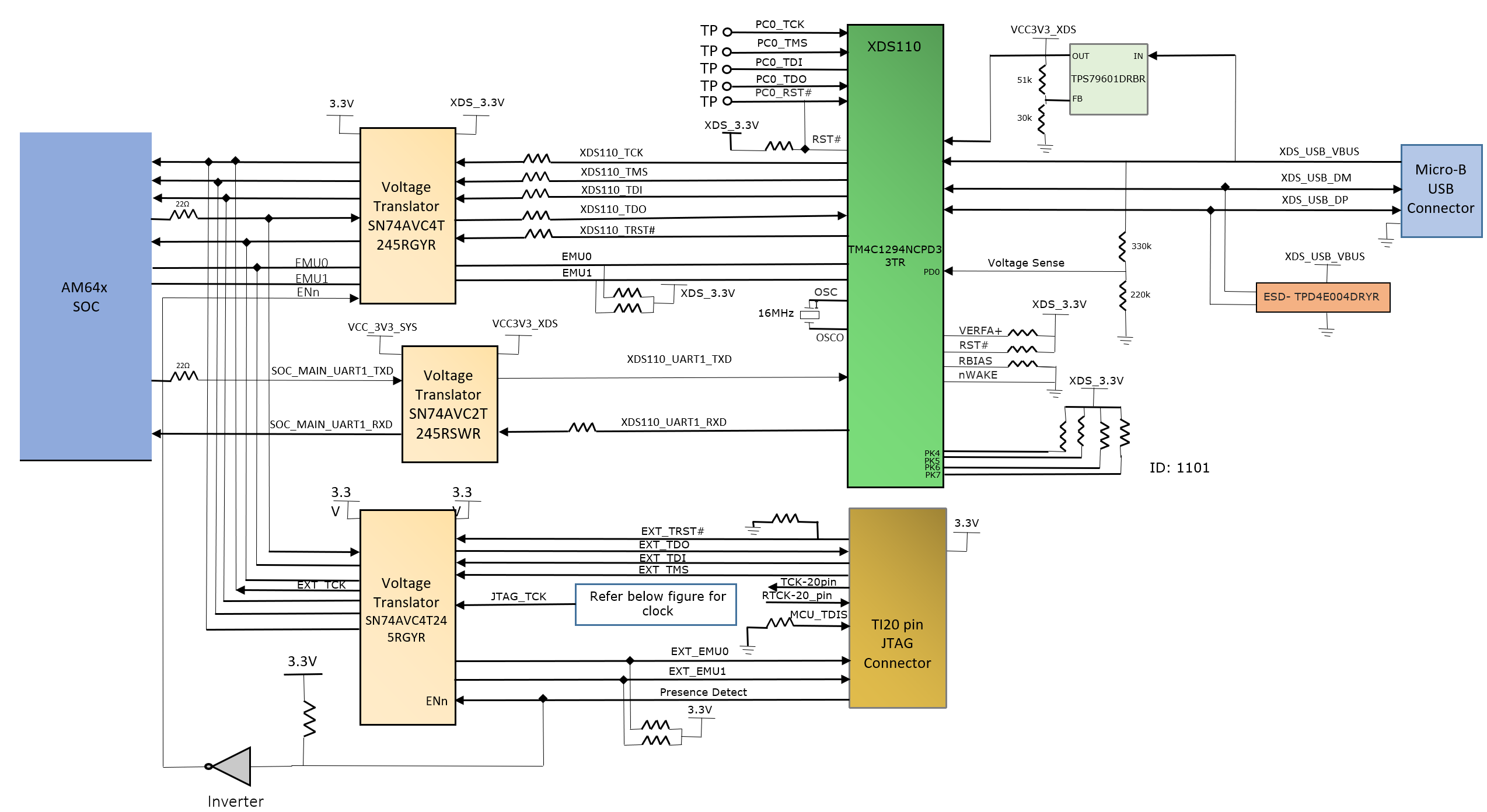
The SKEVM board includes XDS110 class on board emulation and a 20-pin cTI header to support TI internal testing of software builds. The SKEVM board includes the circuitry needed for XDS110 emulation. The connection for the emulator uses an USB2.0 micro-B connector J12 and the circuit acts as a powered USB slave device. The VBUS power from the connector is used to power the emulation circuit such that connection to the emulator is not lost when the power to the EVM is removed. Voltage translation buffers are needed to isolate the XDS110 circuit from the rest of the EVM. Additionally, XDS110 also offers UART to USB signal translation on the same USB port. UART1 of SoC MAIN Domain without flow control is connected to XDS110 UART port via an isolator.
Optionally, JTAG interface on SKEVM is also provided through 20-pin standard JTAG cTI Header J14. This allows the user to connect an external JTAG Emulator cable. Voltage translation buffers are used to isolate the JTAG signals from cTI header from the rest of the EVM. The output from the voltage translators from XDS110 section and cTI Header section is muxed and connected to SoC AM64x JTAG interface. If a connection to the cTI 20-pin JTAG connector is sensed using a present detect circuit, the mux will be set to route the 20-pin signals to the AM64x in place of the on-board emulation circuit.
The pin-outs of cTI 20-pin JTAG connector J14 are given in Table 4-13. An ESD protection part number TPD4E004 is provided on USB signals to steer ESD current pulses to VCC or GND. TPD4E004 protects against ESD pulses up to ±15-kV Human-Body Model (HBM) as specified in IEC 61000-4-2 and provides ±8-kV contact discharge and ±12- kV air-gap discharge.
| Pin No. | Signal | Pin No. | Signal |
|---|---|---|---|
| 1 | JTAG_TMS | 11 | JTAG_cTI_TCK |
| 2 | JTAG_TRST# | 12 | DGND |
| 3 | JTAG_TDI | 13 | JTAG_EMU0 |
| 4 | JTAG_TDIS | 14 | JTAG_EMU1 |
| 5 | VCC_3V3_SYS | 15 | JTAG_EMU_RSTN |
| 6 | NC | 16 | DGND |
| 7 | JTAG_TDO | 17 | NC |
| 8 | SEL_XDS110_INV | 18 | NC |
| 9 | JTAG_cTI_RTCK | 19 | NC |
| 10 | DGND | 20 | DGND |
 Figure 4-5 JTAG Interface