SPRUJ64 September 2022
- Abstract
- Trademarks
- 1Key Features
- 2AM64x SKEVM Overview
- 3Functional Block Diagram
-
4System Description
- 4.1 Clocking
- 4.2 Reset
- 4.3 Power Requirements
- 4.4 Configuration
- 4.5 JTAG
- 4.6 Test Automation
- 4.7 UART Interface
- 4.8 Memory Interfaces
- 4.9 Ethernet Interface
- 4.10 USB 3.0 Interface
- 4.11 PRU Connector
- 4.12 User Expansion Connector
- 4.13 MCU Connector
- 4.14 Interrupt
- 4.15 I2C Interface
- 4.16 IO Expander (GPIOs)
- 5Known Issues and Modifications
- 6Revision History
4.8.1 LPDDR4 Interface
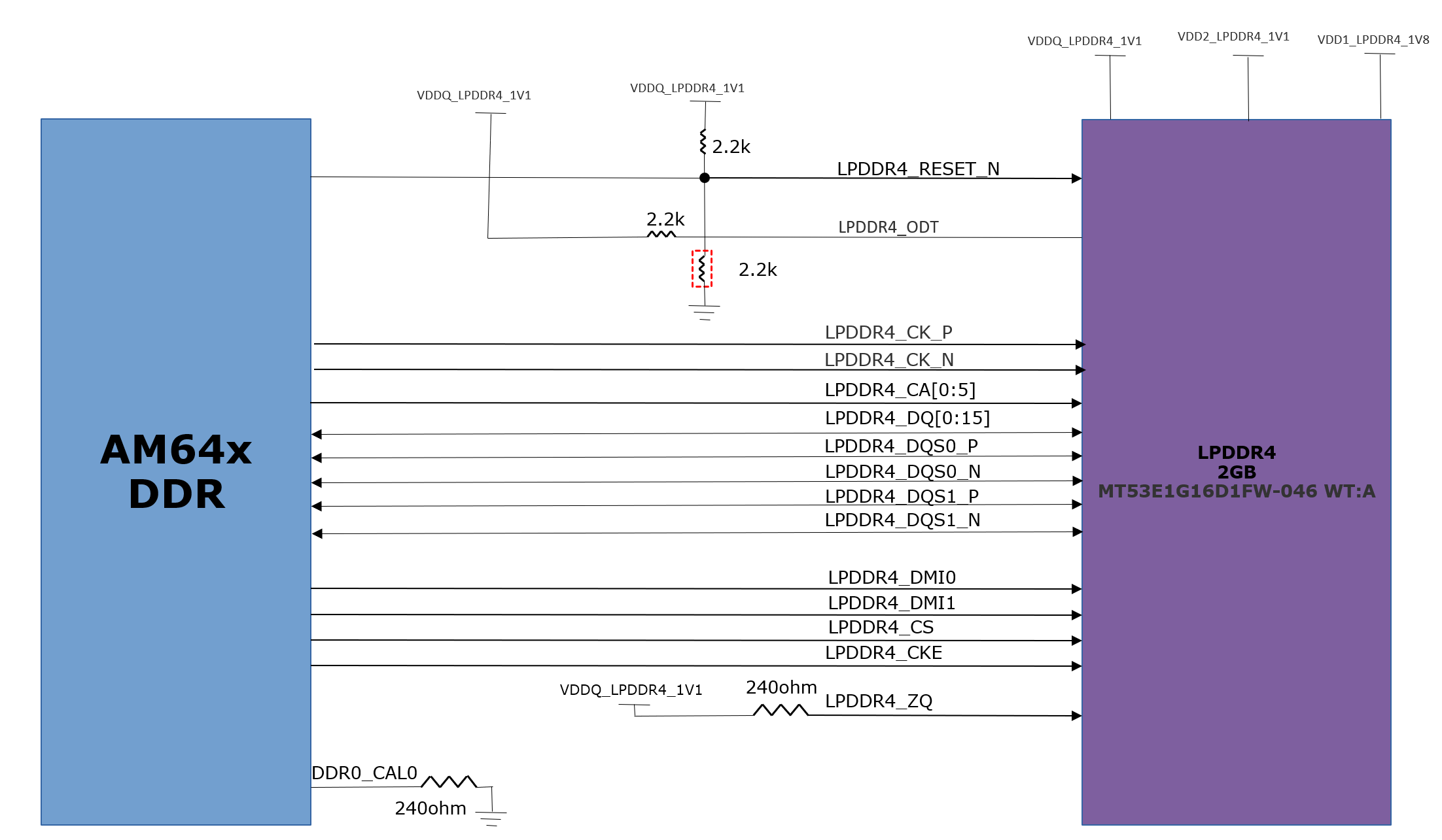
The SK EVM has 2GB, 16-bit wide LPDDR4 memory with operating data rate of 1666 MTps. Micron's MT53E1G16D1FW-046 WT: A is used. The LPDDR memory is mounted on-board (single chip) and requires 1.1 V and thus reduces power demand. The LPDDR4 device requires I/O power and core 2 power of 1.1 V, DRAM activating power supply (core 1) of 1.8 V.
LPDDR4 reset is active high signal, which is controlled by SOC, and the signal is pulled low to set the default active state and a footprint for pull-down is also provided. A 240-Ω resistor is connected from ZQ pin to 1.1-V supply for the LPDDR4 device and the SoC DDR0_CAL pin is grounded.
The ODT (On Die Termination) is applied to DQ, DQS, and DM_n signals. The device is capable of providing three different ODT modes: Nominal, Dynamic, and Park with termination values: RTT (Park), RTT (NOM), and RTT (WR). Figure 4-8 shows the DDR interface between LPDDR4 and AM64x.
 Figure 4-8 LPDDR4 Interface