SPRUJ64 September 2022
- Abstract
- Trademarks
- 1Key Features
- 2AM64x SKEVM Overview
- 3Functional Block Diagram
-
4System Description
- 4.1 Clocking
- 4.2 Reset
- 4.3 Power Requirements
- 4.4 Configuration
- 4.5 JTAG
- 4.6 Test Automation
- 4.7 UART Interface
- 4.8 Memory Interfaces
- 4.9 Ethernet Interface
- 4.10 USB 3.0 Interface
- 4.11 PRU Connector
- 4.12 User Expansion Connector
- 4.13 MCU Connector
- 4.14 Interrupt
- 4.15 I2C Interface
- 4.16 IO Expander (GPIOs)
- 5Known Issues and Modifications
- 6Revision History
4.8.2.3 OSPI Interface
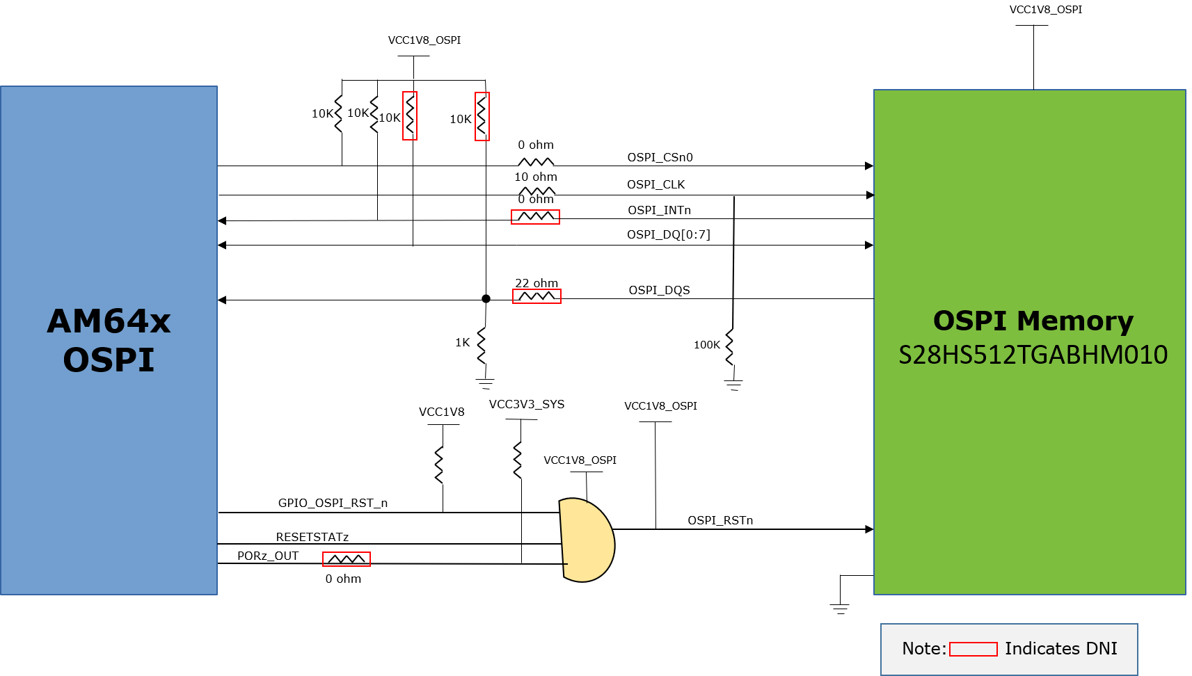
The SK EVM board has a 512-Mbit OSPI memory device of part number S28HS512TGABHM010 from Cypress connected to the OSPI0 interface of the AM64x SOC. The OSPI interface supports memory speed up to 166 MHz. The OSPI flash is powered by 1.8-V IO supply. The 1.8-V supply is provided to both the VCC and VCCQ pins of the flash memory.
The reset for the flash is connected to a circuit that ANDs the RESETSTATz, PORz_OUT, and OSPI0_CSN2 (GPIO_OSPI_RSTn) from SoC. This applies reset for warm and cold reset. A pull-up is provided on GPIO_OSPI_RSTn coming from the SOC pin to set the default active state.
Two signals are routed to OSPI0_DQS:
- OSPI0_DQS from the memory device
- OSPI0_LBCLK from SoC
To route DQS from memory device: DNI R33 and R39.
To route OSPI0_LBCLK from SoC: Mount R33 and R39.
OSPI and QSPI implementation: 0-ohm resistors are provided for DATA [7:0], DQS, INT# and CLK signals. Footprints to mount external pull up resistors are provided on DATA [7:0] to prevent bus floating.
Figure 4-11 shows the OSPI interface block diagram for AM64x SK EVM.
 Figure 4-11 OSPI
Interface