SPRUJ64 September 2022
- Abstract
- Trademarks
- 1Key Features
- 2AM64x SKEVM Overview
- 3Functional Block Diagram
-
4System Description
- 4.1 Clocking
- 4.2 Reset
- 4.3 Power Requirements
- 4.4 Configuration
- 4.5 JTAG
- 4.6 Test Automation
- 4.7 UART Interface
- 4.8 Memory Interfaces
- 4.9 Ethernet Interface
- 4.10 USB 3.0 Interface
- 4.11 PRU Connector
- 4.12 User Expansion Connector
- 4.13 MCU Connector
- 4.14 Interrupt
- 4.15 I2C Interface
- 4.16 IO Expander (GPIOs)
- 5Known Issues and Modifications
- 6Revision History
4.11 PRU Connector
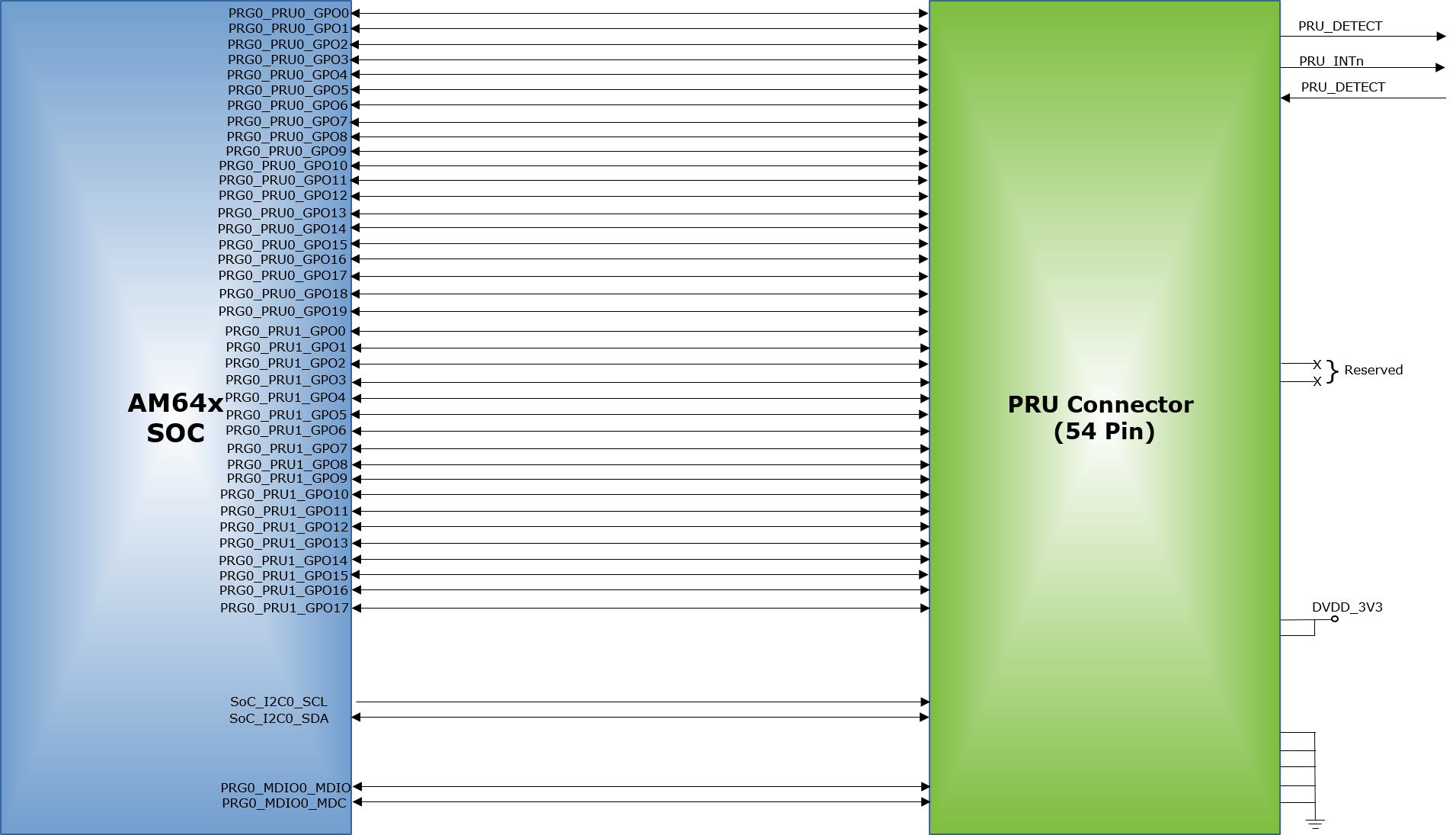
PRU header offers low speed connection to the PRG0 interface. PRU_ICSSG signals from a PRG0 port (PRG0_PRU0 and PRG0_PRU1) are terminated on the PRU expansion connector. PRU0 signals are connected to a 27x2 standard 0.1” spaced 54-pin connector. The connector contains MDIO control signals (2 pins), PRG0_PRU0_GPO [0: 19], PRG0_PRU1_GPO [0: 17], +3.3V PWR (2 pins) and Ground reference (5 pins), DETECT, RESET, INT going to the daughter card and SoC I2C0 lines (2 pins). 3.3 V are current limited to 200 mA. This is achieved by using load switch TPS22902YFPR. Enable for the load switch is controlled by the SoC.
Signals routed from the PRU connector are listed in Table 4-20
| Pin | Net Name | Pin | Net Name |
|---|---|---|---|
| 1 | VCC3V3_PRU | 2 | DGND |
| 3 | PRU_DETECT | 4 | PRU_RESETz |
| 5 | PRU_INTn | 6 | SoC_I2C0_SCL |
| 7 | PRG0_PRU0GPO16 | 8 | SoC_I2C0_SDA |
| 9 | PRG0_MDIO0_MDC | 10 | NC |
| 11 | PRG0_MDIO0_MDIO | 12 | NC |
| 13 | PRG0_PRU0GPO0 | 14 | PRG0_PRU0GPO1 |
| 15 | PRG0_PRU0GPO2 | 16 | PRG0_PRU0GPO3 |
| 17 | PRG0_PRU0GPO4 | 18 | PRG0_PRU0GPO5 |
| 19 | PRG0_PRU0GPO6 | 20 | PRG0_PRU0GPO7 |
| 21 | PRG0_PRU0GPO8 | 22 | PRG0_PRU0GPO9 |
| 23 | PRG0_PRU0GPO10 | 24 | PRG0_PRU0GPO11 |
| 25 | PRG0_PRU0GPO12 | 26 | PRG0_PRU0GPO13 |
| 27 | PRG0_PRU0GPO14 | 28 | PRG0_PRU0GPO15 |
| 29 | DGND | 30 | PRG0_PRU0GPO17 |
| 31 | PRG0_PRU0GPO18 | 32 | PRG0_PRU0GPO19 |
| 33 | DGND | 34 | DGND |
| 35 | PRG0_PRU1GPO0 | 36 | PRG0_PRU1GPO1 |
| 37 | PRG0_PRU1GPO2 | 38 | PRG0_PRU1GPO3 |
| 39 | PRG0_PRU1GPO4 | 40 | PRG0_PRU1GPO5 |
| 41 | PRG0_PRU1GPO6 | 42 | PRG0_PRU1GPO7 |
| 43 | PRG0_PRU1GPO8 | 44 | PRG0_PRU1GPO9 |
| 45 | PRG0_PRU1GPO10 | 46 | PRG0_PRU1GPO11 |
| 47 | PRG0_PRU1GPO12 | 48 | PRG0_PRU1GPO13 |
| 49 | PRG0_PRU1GPO14 | 50 | PRG0_PRU1GPO15 |
| 51 | PRG0_PRU1GPO16 | 52 | PRG0_PRU1GPO17 |
| 53 | DGND | 54 | VCC3V3_PRU |
 Figure 4-18 54-Pin PRU Connector