ZHCSNF1 February 2021 BQ25960
PRODUCTION DATA
- 1 特性
- 2 应用
- 3 说明
- 4 Revision History
- 5 Description (continued)
- 6 Device Comparison Table
- 7 Pin Configuration and Functions
- 8 Specifications
-
9 Detailed Description
- 9.1 Overview
- 9.2 Functional Block Diagram
- 9.3
Feature Description
- 9.3.1 Charging System
- 9.3.2 Battery Charging Profile
- 9.3.3 Device Power Up
- 9.3.4 Device HIZ State
- 9.3.5 Dual Input Bi-Directional Power Path Management
- 9.3.6 Bypass Mode Operation
- 9.3.7 Charging Start-Up
- 9.3.8 Adapter Removal
- 9.3.9 Integrated 16-Bit ADC for Monitoring and Smart Adapter Feedback
- 9.3.10 Device Modes and Protection Status
- 9.3.11 INT Pin, STAT, FLAG, and MASK Registers
- 9.3.12 Dual Charger Operation Using Primary and Secondary Modes
- 9.3.13 CDRVH and CDRVL_ADDRMS Functions
- 9.4 Programming
- 9.5 Register Maps
- 10Application and Implementation
- 11Power Supply Recommendations
- 12Layout
- 13Device and Documentation Support
- 14Mechanical, Packaging, and Orderable Information
9.3.12 Dual Charger Operation Using Primary and Secondary Modes
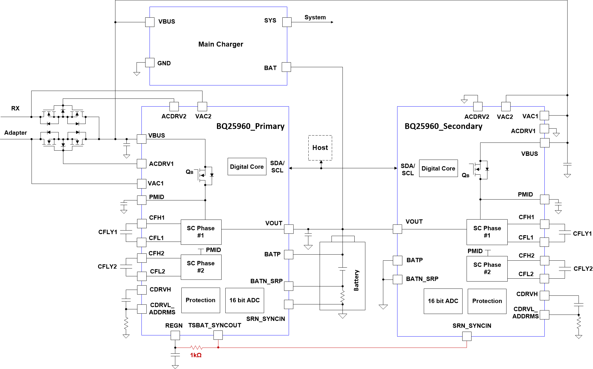
For higher power systems, it is possible to use two devices in dual charger configuration. This allows each device to operate at lower charging current with higher efficiency compared with single device operating at the same total charging current. The CDRVL_ADDRMS pin is used to configure the functionality of the device as Standalone, Primary or Secondary during POR. Refer to Section 9.3.13 for proper setting. When configured as a primary, the TSBAT_SYNCOUT pin functions as SYNCOUT, and the SRN_SYNCIN pin functions as SRN. When configured as a Secondary, the TSBAT_SYNCOUT pin functions as TSBAT, and the SRN_SYNCIN pin functions as SYNCIN. ACDRV1 and ACDRV2 are controlled by the primary, and ACDRV1 and ACDRV2 on the secondary should be grounded. Pull the SYNCIN/SYNCOUT pins to REGN on the primary BQ25960 through a 1-kΩ resistor. The maximum switching frequency in primary and secondary mode is 500 kHz.
The dual charger can operate in Primary and Secondary Mode in Bypass Mode as well. In both Bypass and Switched Cap Mode, the current distribution between the two devices depends on loop impedance and the chargers do not balance it. In order balance the current, the board layout needs to be as symmetrical as possible.
 Figure 9-9 Parallel Operation of BQ25960