ZHCSNF1 February 2021 BQ25960
PRODUCTION DATA
- 1 特性
- 2 应用
- 3 说明
- 4 Revision History
- 5 Description (continued)
- 6 Device Comparison Table
- 7 Pin Configuration and Functions
- 8 Specifications
-
9 Detailed Description
- 9.1 Overview
- 9.2 Functional Block Diagram
- 9.3
Feature Description
- 9.3.1 Charging System
- 9.3.2 Battery Charging Profile
- 9.3.3 Device Power Up
- 9.3.4 Device HIZ State
- 9.3.5 Dual Input Bi-Directional Power Path Management
- 9.3.6 Bypass Mode Operation
- 9.3.7 Charging Start-Up
- 9.3.8 Adapter Removal
- 9.3.9 Integrated 16-Bit ADC for Monitoring and Smart Adapter Feedback
- 9.3.10 Device Modes and Protection Status
- 9.3.11 INT Pin, STAT, FLAG, and MASK Registers
- 9.3.12 Dual Charger Operation Using Primary and Secondary Modes
- 9.3.13 CDRVH and CDRVL_ADDRMS Functions
- 9.4 Programming
- 9.5 Register Maps
- 10Application and Implementation
- 11Power Supply Recommendations
- 12Layout
- 13Device and Documentation Support
- 14Mechanical, Packaging, and Orderable Information
9.3.5.3 Single Input with ACFET1
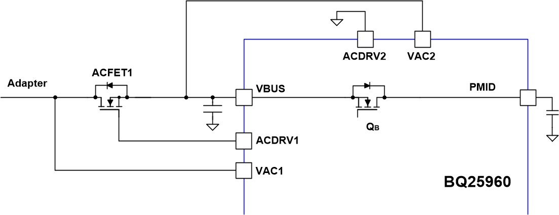
In this scenario, ACFET1 without RBFET1 is populated, but ACFET2-RBFET2 is not. VAC2 is short to VBUS and ACDRV2 is pulled down to ground. The table below summarizes the VAC1/ VAC2, ACDRV1/ACDRV2 connection, register control, and status functions. Use VAC1 for single input configuration.
Table 9-2 Single Input with Single
ACFET1
| INPUT CONFIGURATION | SINGLE INPUT |
|---|---|
| External FET connection | ACFET1, no ACFET2-RBFET2 |
| Input pin connection | VAC1 connected to input source VAC2 short to VBUS |
| ACDRV pin connection | ACDRV1 active ACDRV2 tie to ground |
| ACDRV1_STAT | 1: ACDRV1 is ON 0: ACDRV1 is OFF |
| ACDRV2_STAT | 0 |
| DIS_ACDRV_BOTH | 0: Allow ACDRV1 to turn on if the conditions of ACDRV turn on
are met. 1: Force ACDRV1 OFF |
| ACRB1_CONFIG_STAT | 1 |
| ACRB2_CONFIG_STAT | 0 |
| EN_HIZ | 0: Allow ACDRV1 to turn on if the conditions of ACDRV turn on
are met. 1: Force ACDRV1 OFF |
 Figure 9-4 Single Input with
ACFET1