ZHCSNF1 February 2021 BQ25960
PRODUCTION DATA
- 1 特性
- 2 应用
- 3 说明
- 4 Revision History
- 5 Description (continued)
- 6 Device Comparison Table
- 7 Pin Configuration and Functions
- 8 Specifications
-
9 Detailed Description
- 9.1 Overview
- 9.2 Functional Block Diagram
- 9.3
Feature Description
- 9.3.1 Charging System
- 9.3.2 Battery Charging Profile
- 9.3.3 Device Power Up
- 9.3.4 Device HIZ State
- 9.3.5 Dual Input Bi-Directional Power Path Management
- 9.3.6 Bypass Mode Operation
- 9.3.7 Charging Start-Up
- 9.3.8 Adapter Removal
- 9.3.9 Integrated 16-Bit ADC for Monitoring and Smart Adapter Feedback
- 9.3.10 Device Modes and Protection Status
- 9.3.11 INT Pin, STAT, FLAG, and MASK Registers
- 9.3.12 Dual Charger Operation Using Primary and Secondary Modes
- 9.3.13 CDRVH and CDRVL_ADDRMS Functions
- 9.4 Programming
- 9.5 Register Maps
- 10Application and Implementation
- 11Power Supply Recommendations
- 12Layout
- 13Device and Documentation Support
- 14Mechanical, Packaging, and Orderable Information
10.2.1.3 Application Curves
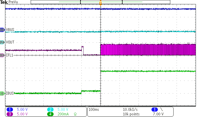 Figure 10-3 Switched Cap Mode Power Up
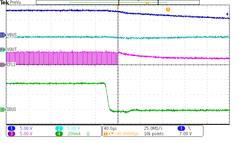 Figure 10-5 Adapter Unplug in Switched Cap Mode
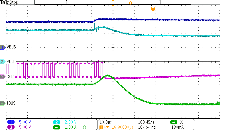 Figure 10-7 VBUSOVP in Switched Cap Mode
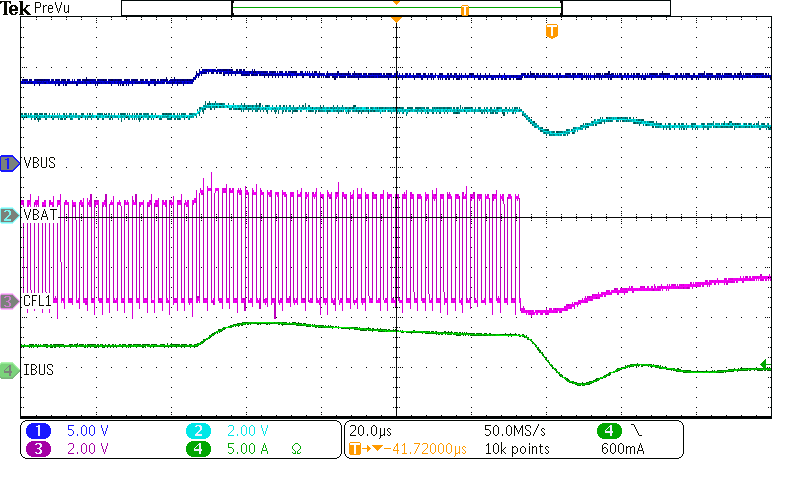 Figure 10-9 IBUSOCP in Switched Cap Mode
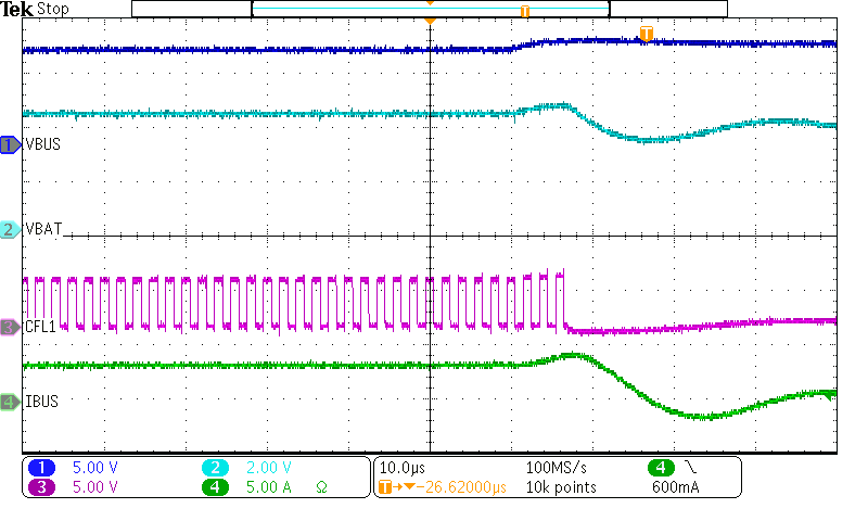 Figure 10-11
VBATOVP in Switched Cap Mode
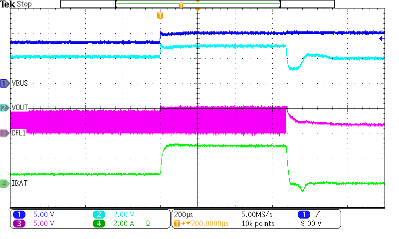 Figure 10-13 IBATOCP in Switched Cap Mode
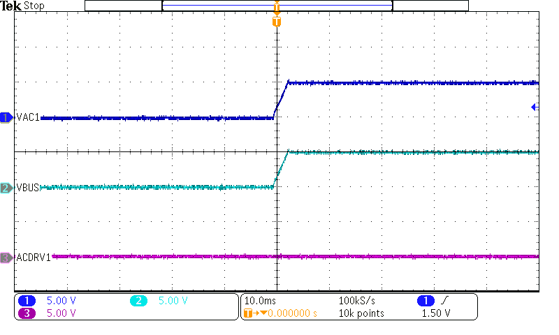
| VAC1 and VAC2 short to VBUS, ACDRV1 and ACDRV2 short to ground |
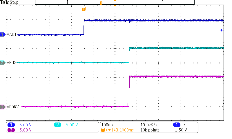
| VAC1 connected to input source 1, VBUS connected to input source 2, VAC2 short to VBUS, ACDRV1 active, ACDRV2 short to ground |
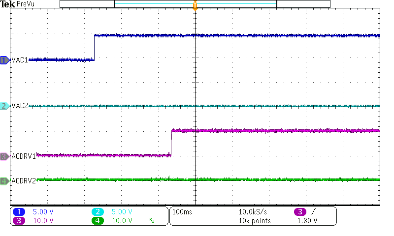
| VAC1 connected to input source 1, VAC2 connected to input source 2, ACDRV1 and ACDRV2 active |
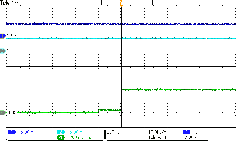 Figure 10-4 Bypass Mode Power Up
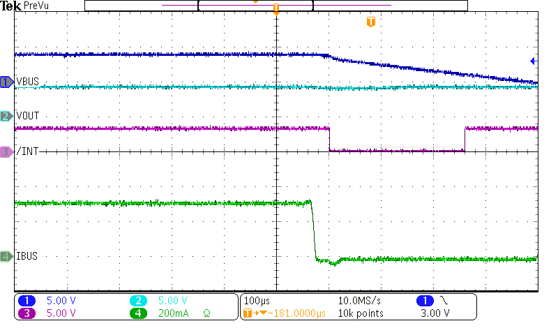 Figure 10-6 Adapter Unplug in Bypass Mode
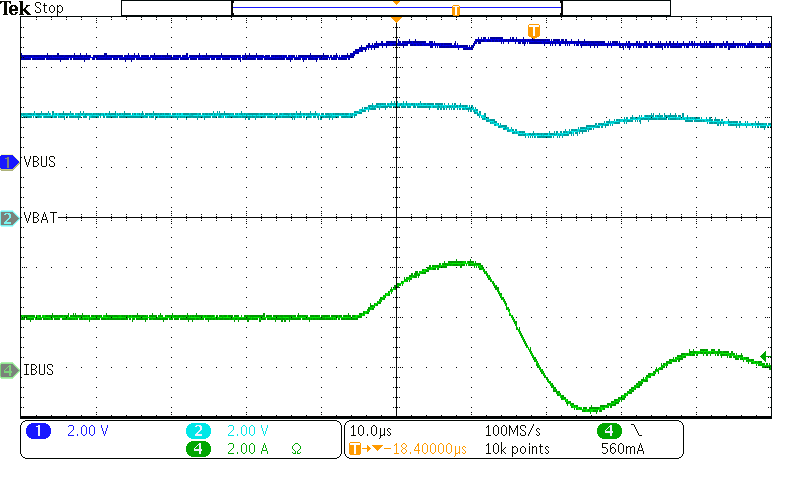 Figure 10-8 VBUSOVP in Bypass Mode
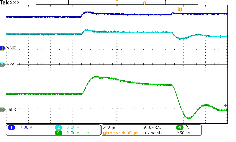 Figure 10-10 IBUSOCP in Bypass Mode
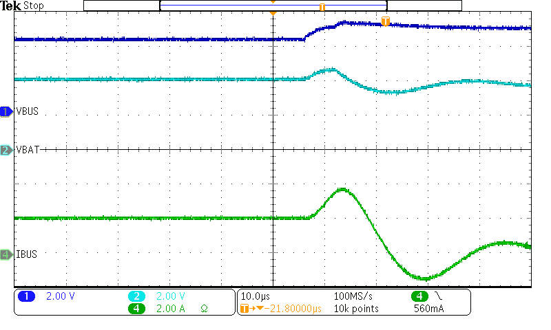 Figure 10-12 VBATOVP in Bypass Mode
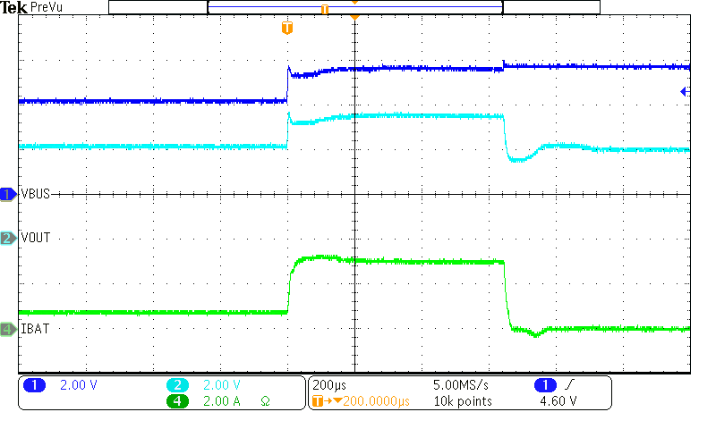 Figure 10-14 IBATOCP in Bypass Mode
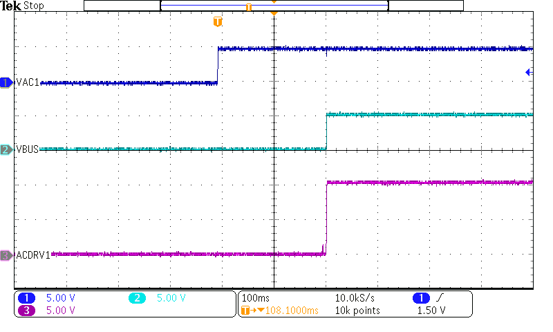
| VAC1 connected to input source, VAC2 short to VBUS, ACDRV1 active, ACDRV2 short to ground |
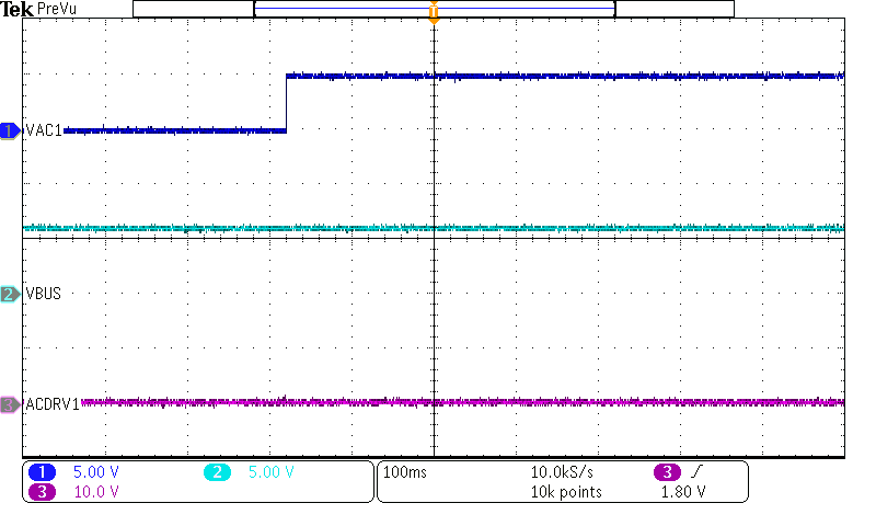
| VAC1 connected to input source 1, VBUS connected to input source 2, VAC2 short to VBUS, ACDRV1 active, ACDRV2 short to ground |
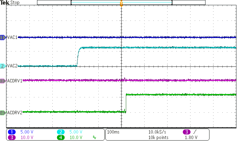
| VAC1 connected to input source 1, VAC2 connected to input source 2, ACDRV1 and ACumDRV2 active |