ZHCSNF1 February 2021 BQ25960
PRODUCTION DATA
- 1 特性
- 2 应用
- 3 说明
- 4 Revision History
- 5 Description (continued)
- 6 Device Comparison Table
- 7 Pin Configuration and Functions
- 8 Specifications
-
9 Detailed Description
- 9.1 Overview
- 9.2 Functional Block Diagram
- 9.3
Feature Description
- 9.3.1 Charging System
- 9.3.2 Battery Charging Profile
- 9.3.3 Device Power Up
- 9.3.4 Device HIZ State
- 9.3.5 Dual Input Bi-Directional Power Path Management
- 9.3.6 Bypass Mode Operation
- 9.3.7 Charging Start-Up
- 9.3.8 Adapter Removal
- 9.3.9 Integrated 16-Bit ADC for Monitoring and Smart Adapter Feedback
- 9.3.10 Device Modes and Protection Status
- 9.3.11 INT Pin, STAT, FLAG, and MASK Registers
- 9.3.12 Dual Charger Operation Using Primary and Secondary Modes
- 9.3.13 CDRVH and CDRVL_ADDRMS Functions
- 9.4 Programming
- 9.5 Register Maps
- 10Application and Implementation
- 11Power Supply Recommendations
- 12Layout
- 13Device and Documentation Support
- 14Mechanical, Packaging, and Orderable Information
9.3.2 Battery Charging Profile
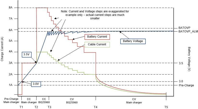
The system will have a specific battery charging profile that is unique due to the switched cap architecture. The charging will be controlled by the main charger such as the BQ2561x or BQ2589x until ystem voltage reaches minimum system regulation voltage VSYSMIN. Once the battery voltage reaches VSYSMIN (3.5 V), the adapter can negotiate for a higher bus voltage, enable BQ25960 charging, and regulate the current on VBUS to charge the battery. In the CC phase, the protection in BQ25960 will not regulate the battery voltage, but will provide feedback to the system to increase and decrease current as needed, as well as disable the blocking and switching FETs if the voltage is exceeded. Once the CV point is reached, the BQ25960 will provide feedback to the adapter to reduce the current, effectively tapering the current until a point where the main charger takes over again. The BQ25960 can operate as long as input current is above the BUSUCP threshold.
 Figure 9-2 BQ25960 System Charging
Profile