ZHCSNF1 February 2021 BQ25960
PRODUCTION DATA
- 1 特性
- 2 应用
- 3 说明
- 4 Revision History
- 5 Description (continued)
- 6 Device Comparison Table
- 7 Pin Configuration and Functions
- 8 Specifications
-
9 Detailed Description
- 9.1 Overview
- 9.2 Functional Block Diagram
- 9.3
Feature Description
- 9.3.1 Charging System
- 9.3.2 Battery Charging Profile
- 9.3.3 Device Power Up
- 9.3.4 Device HIZ State
- 9.3.5 Dual Input Bi-Directional Power Path Management
- 9.3.6 Bypass Mode Operation
- 9.3.7 Charging Start-Up
- 9.3.8 Adapter Removal
- 9.3.9 Integrated 16-Bit ADC for Monitoring and Smart Adapter Feedback
- 9.3.10 Device Modes and Protection Status
- 9.3.11 INT Pin, STAT, FLAG, and MASK Registers
- 9.3.12 Dual Charger Operation Using Primary and Secondary Modes
- 9.3.13 CDRVH and CDRVL_ADDRMS Functions
- 9.4 Programming
- 9.5 Register Maps
- 10Application and Implementation
- 11Power Supply Recommendations
- 12Layout
- 13Device and Documentation Support
- 14Mechanical, Packaging, and Orderable Information
9.3.6 Bypass Mode Operation
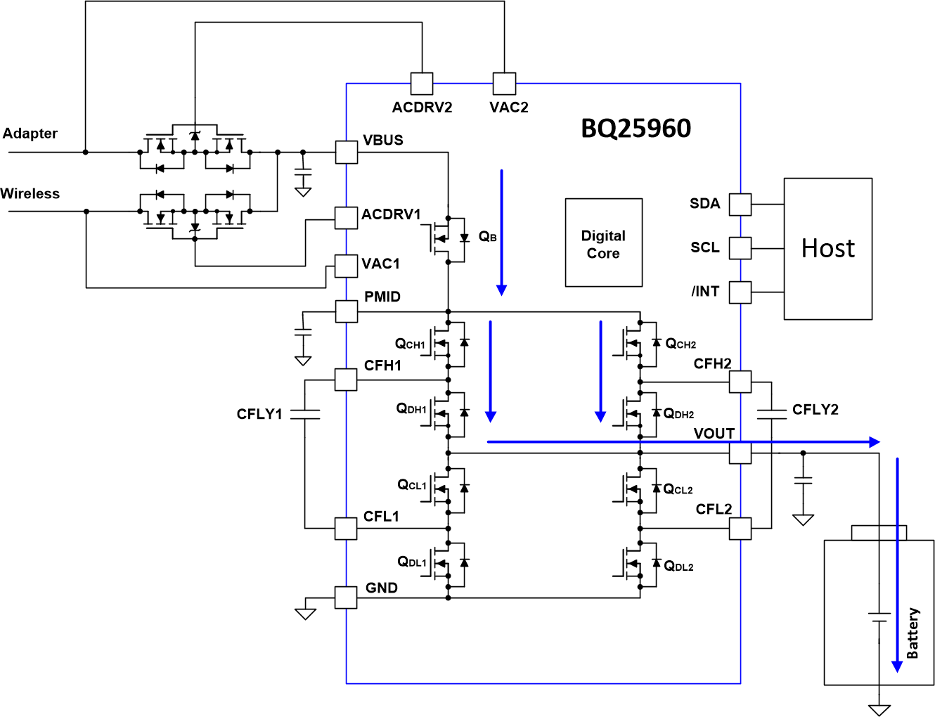
When host determines the adapter support bypass mode charging, the device can enable Bypass mode by setting EN_BYPASS=1. Blocking FET (QB) and four high side switching FET (QCH1 and QDH1/ QCH2 and QDH2) are turned on to charge from adapter to battery. During Bypass Mode, when fault occurs, CHG_EN is cleared but EN_BYPASS stays ‘1’.
 Figure 9-7 BQ25960 Bypass Mode
To change from Bypass Mode to Switched Cap Mode or from Switched Cap to Bypass Mode, the host would first set CHG_EN=0 to stop the converter and then set EN_BYPASS to desired value. The host sets desired protection threshold based on the selected operation modes and then host enables charge by setting CHG_EN=1.