ZHCSNF1 February 2021 BQ25960
PRODUCTION DATA
- 1 特性
- 2 应用
- 3 说明
- 4 Revision History
- 5 Description (continued)
- 6 Device Comparison Table
- 7 Pin Configuration and Functions
- 8 Specifications
-
9 Detailed Description
- 9.1 Overview
- 9.2 Functional Block Diagram
- 9.3
Feature Description
- 9.3.1 Charging System
- 9.3.2 Battery Charging Profile
- 9.3.3 Device Power Up
- 9.3.4 Device HIZ State
- 9.3.5 Dual Input Bi-Directional Power Path Management
- 9.3.6 Bypass Mode Operation
- 9.3.7 Charging Start-Up
- 9.3.8 Adapter Removal
- 9.3.9 Integrated 16-Bit ADC for Monitoring and Smart Adapter Feedback
- 9.3.10 Device Modes and Protection Status
- 9.3.11 INT Pin, STAT, FLAG, and MASK Registers
- 9.3.12 Dual Charger Operation Using Primary and Secondary Modes
- 9.3.13 CDRVH and CDRVL_ADDRMS Functions
- 9.4 Programming
- 9.5 Register Maps
- 10Application and Implementation
- 11Power Supply Recommendations
- 12Layout
- 13Device and Documentation Support
- 14Mechanical, Packaging, and Orderable Information
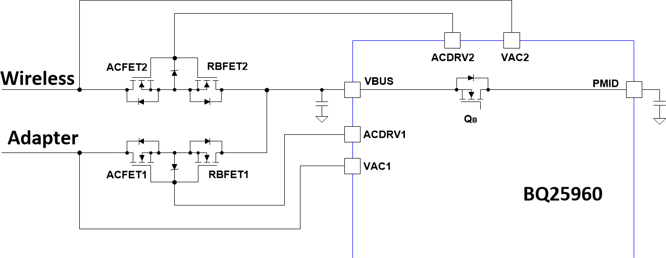
9.3.5.5 Dual Input with ACFET1-RBFET1 and ACFET2-RBFET2
In this scenario, both ACFET1-RBFET1 and ACFET2-RBFET2 are populated and the device supports dual input. The table below summarizes the connection, register control and status functions. Connect input with high OVP threshold to VAC1.
| INPUT CONFIGURATION | DUAL INPUT |
|---|---|
| External FET connection | ACFET1-RBFET1, ACFET1-RBFET2 |
| Input pin connection |
VAC1 connected to input source 1 VAC2 connected to input source 2 No input source allowed to connect to VBUS |
| ACDRV pin connection | ACDRV1 and ACDRV2 active |
| ACDRV1_STAT |
0: ACDRV1 OFF 1: ACDRV1 ON Once device is in dual input configuration with ACFET1-RBFET1 and ACFET2-RBFET2, the host can use this bit to swap the input between VAC1 and VAC2 if both VAC1 and VAC2 are valid. |
| ACDRV2_STAT |
0: ACDRV2 OFF 1: ACDRV2 ON Once device is in dual input configuration with ACFET1-RBFET1 and ACFET2-RBFET2, the host can use this bit to swap the input between VAC1 and VAC2 if both VAC1 and VAC2 are valid. |
| DIS_ACDRV_BOTH | 0: Allow ACDRV to turn on. By default, ACDRV1 is turned on if the conditions of ACDRV turn on are met, ACDRV1_STAT=1 and ACDRV2_STAT =0. In On-The-GO (OTG) or Reverse TX Mode, refer to OTG and Reverse TX Mode Operation session for turn on precedence. 1: Force both ACDRV to turn off, both ACDRV1_STAT and ACDRV2_STAT become 0. |
| ACRB1_CONFIG_STAT | 1 |
| ACRB2_CONFIG_STAT | 1 |
| EN_HIZ | 0: Allow ACDRV to turn on for the port w/ VAC present if the conditions of ACDRV turn on are met. ACDRV1 is turned on since VAC1 is the primary input source when both VAC1 and VAC2 present and the turn on conditions are met. 1: Turns off both ACDRV |
 Figure 9-6 Two Inputs with ACFET-RBFET1 and
ACFET-RBFET2