ZHCSL05C October 2019 – October 2023 TPS65313-Q1
PRODUCTION DATA
- 1
- 1 特性
- 2 应用
- 3 说明
- 4 器件功能方框图
- 5 Revision History
- 6 说明(续)
- 7 Device Option Table
- 8 Pin Configuration and Functions
-
9 Specifications
- 9.1 Absolute Maximum Ratings
- 9.2 ESD Ratings
- 9.3 Recommended Operating Conditions
- 9.4 Thermal Information
- 9.5 Power-On-Reset, Current Consumption, and State Timeout Characteristics
- 9.6 PLL/Oscillator and SYNC_IN Pin Characteristics
- 9.7 Wide-VIN Synchronous Buck Regulator (Wide-VIN BUCK) Characteristics
- 9.8 Low-Voltage Synchronous Buck Regulator (LV BUCK) Characteristics
- 9.9 Synchronous Boost Converter (BOOST) Characteristics
- 9.10 Internal Voltage Regulator (VREG) Characteristics
- 9.11 Voltage Monitors for Regulators Characteristics
- 9.12 External General Purpose Voltage Monitor Characteristics
- 9.13 VIN and VIN_SAFE Under-Voltage and Over-Voltage Warning Characteristics
- 9.14 WAKE Input Characteristics
- 9.15 NRES (nRESET) Output Characteristics
- 9.16 ENDRV/nIRQ Output Characteristics
- 9.17 Analog DIAG_OUT
- 9.18 Digital INPUT/OUTPUT IOs (SPI Interface IOs, DIAG_OUT/SYNC_OUT, MCU_ERROR)
- 9.19 BUCK1, BUCK2, BOOST Thermal Shutdown / Over Temperature Protection Characteristics
- 9.20 PGNDx Loss Detection Characteristics
- 9.21 SPI Timing Requirements
- 9.22 SPI Characteristics
- 9.23 Typical Characteristics
- 10Parameter Measurement Information
-
11Detailed Description
- 11.1 Overview
- 11.2 Functional Block Diagram
- 11.3
Wide-VIN Buck Regulator (BUCK1)
- 11.3.1 Fixed-Frequency Voltage-Mode Step-Down Regulator
- 11.3.2 Operation
- 11.3.3 Voltage Monitoring (Monitoring and Protection)
- 11.3.4 Overcurrent Protection (Monitoring and Protection)
- 11.3.5 Thermal Warning and Shutdown Protection (Monitoring and Protection)
- 11.3.6 Overvoltage Protection (OVP) (Monitoring and Protection)
- 11.3.7 Extreme Overvoltage Protection (EOVP) (Monitoring and Protection)
- 11.4
Low-Voltage Buck Regulator (BUCK2)
- 11.4.1 Fixed-Frequency Peak-Current Mode Step-Down Regulator
- 11.4.2 Operation
- 11.4.3 Output Voltage Monitoring (Monitoring and Protection)
- 11.4.4 Overcurrent Protection (Monitoring and Protection)
- 11.4.5 Thermal Sensor Warning and Thermal Shutdown Protection (Monitoring and Protection)
- 11.4.6 Overvoltage Protection (OVP) (Monitoring and Protection)
- 11.5 Low-Voltage Boost Converter (BOOST)
- 11.6 VREG Regulator
- 11.7
BUCK1, BUCK2, and BOOST Switching Clocks and Synchronization (SYNC_IN) Clock
- 11.7.1 Internal fSW Clock Configuration (fSW Derived from an Internal Oscillator)
- 11.7.2 BUCK1 Switching Clock-Monitor Error (Internal fSW Clock Configuration)
- 11.7.3 BUCK2 Switching Clock-Monitor Error (Internal fSW Clock Configuration)
- 11.7.4 BOOST Switching Clock-Monitor Error (Internal fSW Clock Configuration)
- 11.7.5 External fSW Clock Configuration (fSW Derived from SYNC_IN and PLL Clocks)
- 11.8 BUCK1, BUCK2, and BOOST Switching-Clock Spread-Spectrum Modulation
- 11.9
Monitoring, Protection and Diagnostics Overview
- 11.9.1 Safety Functions and Diagnostic Overview
- 11.9.2 Supply Voltage Monitor (VMON)
- 11.9.3 Clock Monitors
- 11.9.4 Analog Built-In Self-Test
- 11.9.5 Logic Built-In Self-Test
- 11.9.6 Junction Temperature Monitors
- 11.9.7 Current Limit
- 11.9.8 Loss of Ground (GND)
- 11.9.9 Diagnostic Output Pin (DIAG_OUT)
- 11.9.10 Watchdog
- 11.9.11 MCU Error Signal Monitor
- 11.9.12 NRES Driver
- 11.9.13 ENDRV/nIRQ Driver
- 11.9.14 CRC Protection for the Device Configuration Registers
- 11.9.15 CRC Protection for the Device EEPROM Registers
- 11.10 General-Purpose External Supply Voltage Monitors
- 11.11 Analog Wake-up and Failure Latch
- 11.12 Power-Up and Power-Down Sequences
- 11.13 Device Fail-Safe State Controller (Monitoring and Protection)
- 11.14 Wakeup
- 11.15 Serial Peripheral Interface (SPI)
- 11.16 Register Maps
-
12Applications, Implementation, and Layout
- 12.1 Application Information
- 12.2
Typical Application
- 12.2.1 Design Requirements
- 12.2.2
Detailed Design Procedure
- 12.2.2.1 Selecting the BUCK1, BUCK2, and BOOST Output Voltages
- 12.2.2.2 Selecting the BUCK1, BUCK2, and BOOST Inductors
- 12.2.2.3 Selecting the BUCK1 and BUCK2 Output Capacitors
- 12.2.2.4 Selecting the BOOST Output Capacitors
- 12.2.2.5 Input Filter Capacitor Selection for BUCK1, BUCK2, and BOOST
- 12.2.2.6 Input Filter Capacitors on AVIN and VIN_SAFE Pins
- 12.2.2.7 Bootstrap Capacitor Selection
- 12.2.2.8 Internal Linear Regulator (VREG) Output Capacitor Selection
- 12.2.2.9 EXTSUP Pin
- 12.2.2.10 WAKE Input Pin
- 12.2.2.11 VIO Supply Pin
- 12.2.2.12 External General-Purpose Voltage Monitor Input Pins (EXT_VSENSE1 and EXT_VSENSE2)
- 12.2.2.13 SYNC_IN Pin
- 12.2.2.14 MCU_ERR Pin
- 12.2.2.15 NRES Pin
- 12.2.2.16 ENDRV/nIRQ Pin
- 12.2.2.17 DIAG_OUT Pin
- 12.2.2.18 SPI Pins (NCS,SCK, SDI, SDO)
- 12.2.2.19 PBKGx, AGND, DGND, and PGNDx Pins
- 12.2.2.20 Calculations for Power Dissipation and Junction Temperature
- 12.2.3 Application Curves
- 12.2.4 Layout
- 12.3 Power Supply Coupling and Bulk Capacitors
- 13Device and Documentation Support
- 14Mechanical, Packaging, and Orderable Information
12.2.2.3 Selecting the BUCK1 and BUCK2 Output Capacitors
The minimum output capacitance for each regulator is 25 µF and the maximum output capacitance is defined as 100 µF. X7R-type, low-ESR ceramic capacitors are recommended. The minimum and maximum capacitance values specified are the effective capacitance values after considering all the tolerances, voltage derating, and aging effects. Therefore, users must use the value that is higher than the specified value to accommodate for these variations. Select the output capacitor value to be 1.5 times the minimum required capacitance value. The output capacitance range allows users to optimize the output voltage ripple and load transient performance according to their application conditions. Selecting the output capacitance value within the specified range is important to meet the stability requirements of the regulators. Stability performance must be measured on the application board to make sure that regulators are stable for the selected output capacitor.
Use Equation 6 to calculate the output capacitance (COUT) value based on the load transient requirements.
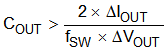
where
- ΔIOUT is the change in output current.
- fSW is the switching frequency of the regulator.
- ΔVOUT is the allowable change in the output voltage.
Use Equation 7 to calculate the peak-to-peak output voltage ripple.
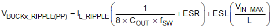
where
- VBUCKx_RIPPLE(PP) is the peak-to-peak-output voltage ripple of the buck regulator.
- IL_RIPPLE is the inductor ripple current (A).
- ESR is the equivalent series resistance of the output capacitor (Ω).
- ESL is the equivalent series inductance of the output capacitor (H).
- VIN_MAX is the maximum input voltage (V).
- L is the value of the inductor (H).
For this example, the BUCK1 voltage is 3.3 V with a 2% change in the output voltage for a load step from 0 A to 2 A. The resulting value of the BUCK1 output capacitance is approximately 28 µF. Considering the capacitor tolerances, derating, and aging effects, two 22-µF, 10-V rating, X7R-type capacitors (GCM31CR71A226KE02 from Murata) are used.
For this example, the calculated BUCK1 output voltage ripple is approximately 11 mVPP for a typical 44-µF capacitor with 3-mΩ effective ESR, 1-nH ESL, 18-V input voltage, 3.3-V output voltage, 3-A maximum load current, and an inductor ripple current that is approximately 20% of the maximum load current.
For this example, the BUCK2 voltage is 1.8 V with a 2 % change in the output voltage for a load step from 0 A to 1 A. The resulting value of the BUCK2 output capacitance is approximately 25 µF. Considering the capacitor tolerances, derating, and aging effects, two 22-µF, 10-V rating, X7R-type capacitors (GCM31CR71A226KE02 from Murata) are used.
For this example, the calculated BUCK2 output voltage ripple is approximately 5 mVPP for a typical 44-µF capacitor with 3-mΩ effective ESR, 1-nH ESL, 3.3-V input voltage, 1.8-V output voltage , 1-µH inductor, 2-A maximum load current, and an inductor ripple current that is approximately 20% of the maximum load current.