ZHCSL05C October 2019 – October 2023 TPS65313-Q1
PRODUCTION DATA
- 1
- 1 特性
- 2 应用
- 3 说明
- 4 器件功能方框图
- 5 Revision History
- 6 说明(续)
- 7 Device Option Table
- 8 Pin Configuration and Functions
-
9 Specifications
- 9.1 Absolute Maximum Ratings
- 9.2 ESD Ratings
- 9.3 Recommended Operating Conditions
- 9.4 Thermal Information
- 9.5 Power-On-Reset, Current Consumption, and State Timeout Characteristics
- 9.6 PLL/Oscillator and SYNC_IN Pin Characteristics
- 9.7 Wide-VIN Synchronous Buck Regulator (Wide-VIN BUCK) Characteristics
- 9.8 Low-Voltage Synchronous Buck Regulator (LV BUCK) Characteristics
- 9.9 Synchronous Boost Converter (BOOST) Characteristics
- 9.10 Internal Voltage Regulator (VREG) Characteristics
- 9.11 Voltage Monitors for Regulators Characteristics
- 9.12 External General Purpose Voltage Monitor Characteristics
- 9.13 VIN and VIN_SAFE Under-Voltage and Over-Voltage Warning Characteristics
- 9.14 WAKE Input Characteristics
- 9.15 NRES (nRESET) Output Characteristics
- 9.16 ENDRV/nIRQ Output Characteristics
- 9.17 Analog DIAG_OUT
- 9.18 Digital INPUT/OUTPUT IOs (SPI Interface IOs, DIAG_OUT/SYNC_OUT, MCU_ERROR)
- 9.19 BUCK1, BUCK2, BOOST Thermal Shutdown / Over Temperature Protection Characteristics
- 9.20 PGNDx Loss Detection Characteristics
- 9.21 SPI Timing Requirements
- 9.22 SPI Characteristics
- 9.23 Typical Characteristics
- 10Parameter Measurement Information
-
11Detailed Description
- 11.1 Overview
- 11.2 Functional Block Diagram
- 11.3
Wide-VIN Buck Regulator (BUCK1)
- 11.3.1 Fixed-Frequency Voltage-Mode Step-Down Regulator
- 11.3.2 Operation
- 11.3.3 Voltage Monitoring (Monitoring and Protection)
- 11.3.4 Overcurrent Protection (Monitoring and Protection)
- 11.3.5 Thermal Warning and Shutdown Protection (Monitoring and Protection)
- 11.3.6 Overvoltage Protection (OVP) (Monitoring and Protection)
- 11.3.7 Extreme Overvoltage Protection (EOVP) (Monitoring and Protection)
- 11.4
Low-Voltage Buck Regulator (BUCK2)
- 11.4.1 Fixed-Frequency Peak-Current Mode Step-Down Regulator
- 11.4.2 Operation
- 11.4.3 Output Voltage Monitoring (Monitoring and Protection)
- 11.4.4 Overcurrent Protection (Monitoring and Protection)
- 11.4.5 Thermal Sensor Warning and Thermal Shutdown Protection (Monitoring and Protection)
- 11.4.6 Overvoltage Protection (OVP) (Monitoring and Protection)
- 11.5 Low-Voltage Boost Converter (BOOST)
- 11.6 VREG Regulator
- 11.7
BUCK1, BUCK2, and BOOST Switching Clocks and Synchronization (SYNC_IN) Clock
- 11.7.1 Internal fSW Clock Configuration (fSW Derived from an Internal Oscillator)
- 11.7.2 BUCK1 Switching Clock-Monitor Error (Internal fSW Clock Configuration)
- 11.7.3 BUCK2 Switching Clock-Monitor Error (Internal fSW Clock Configuration)
- 11.7.4 BOOST Switching Clock-Monitor Error (Internal fSW Clock Configuration)
- 11.7.5 External fSW Clock Configuration (fSW Derived from SYNC_IN and PLL Clocks)
- 11.8 BUCK1, BUCK2, and BOOST Switching-Clock Spread-Spectrum Modulation
- 11.9
Monitoring, Protection and Diagnostics Overview
- 11.9.1 Safety Functions and Diagnostic Overview
- 11.9.2 Supply Voltage Monitor (VMON)
- 11.9.3 Clock Monitors
- 11.9.4 Analog Built-In Self-Test
- 11.9.5 Logic Built-In Self-Test
- 11.9.6 Junction Temperature Monitors
- 11.9.7 Current Limit
- 11.9.8 Loss of Ground (GND)
- 11.9.9 Diagnostic Output Pin (DIAG_OUT)
- 11.9.10 Watchdog
- 11.9.11 MCU Error Signal Monitor
- 11.9.12 NRES Driver
- 11.9.13 ENDRV/nIRQ Driver
- 11.9.14 CRC Protection for the Device Configuration Registers
- 11.9.15 CRC Protection for the Device EEPROM Registers
- 11.10 General-Purpose External Supply Voltage Monitors
- 11.11 Analog Wake-up and Failure Latch
- 11.12 Power-Up and Power-Down Sequences
- 11.13 Device Fail-Safe State Controller (Monitoring and Protection)
- 11.14 Wakeup
- 11.15 Serial Peripheral Interface (SPI)
- 11.16 Register Maps
-
12Applications, Implementation, and Layout
- 12.1 Application Information
- 12.2
Typical Application
- 12.2.1 Design Requirements
- 12.2.2
Detailed Design Procedure
- 12.2.2.1 Selecting the BUCK1, BUCK2, and BOOST Output Voltages
- 12.2.2.2 Selecting the BUCK1, BUCK2, and BOOST Inductors
- 12.2.2.3 Selecting the BUCK1 and BUCK2 Output Capacitors
- 12.2.2.4 Selecting the BOOST Output Capacitors
- 12.2.2.5 Input Filter Capacitor Selection for BUCK1, BUCK2, and BOOST
- 12.2.2.6 Input Filter Capacitors on AVIN and VIN_SAFE Pins
- 12.2.2.7 Bootstrap Capacitor Selection
- 12.2.2.8 Internal Linear Regulator (VREG) Output Capacitor Selection
- 12.2.2.9 EXTSUP Pin
- 12.2.2.10 WAKE Input Pin
- 12.2.2.11 VIO Supply Pin
- 12.2.2.12 External General-Purpose Voltage Monitor Input Pins (EXT_VSENSE1 and EXT_VSENSE2)
- 12.2.2.13 SYNC_IN Pin
- 12.2.2.14 MCU_ERR Pin
- 12.2.2.15 NRES Pin
- 12.2.2.16 ENDRV/nIRQ Pin
- 12.2.2.17 DIAG_OUT Pin
- 12.2.2.18 SPI Pins (NCS,SCK, SDI, SDO)
- 12.2.2.19 PBKGx, AGND, DGND, and PGNDx Pins
- 12.2.2.20 Calculations for Power Dissipation and Junction Temperature
- 12.2.3 Application Curves
- 12.2.4 Layout
- 12.3 Power Supply Coupling and Bulk Capacitors
- 13Device and Documentation Support
- 14Mechanical, Packaging, and Orderable Information
12.2.2.20.2 Device Power Dissipation Estimation
The power dissipation of the device can be estimated by adding the power dissipation of each regulator. The power dissipation of each regulator can be estimated based on the measured efficiency of each regulator. The measured efficiency of the regulator consists of device power losses and inductor power losses. To estimate the power dissipation within the device, the power dissipation of the inductor should be subtracted from the total regulator power dissipation that is calculated based on the efficiency measurement.
Use Equation 16 to estimate the total regulator power dissipation for the BUCK1 regulator, BUCK2 regulator, and BOOST converter.
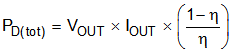
where
- PD(tot) is the total power dissipation of the BUCK1 regulator, BUCK2 regulator, or BOOST converter including inductor power dissipation.
- VOUT is the output voltage of the regulator.
- IOUT is the output current of the regulator.
- η is the efficiency of the regulator based on measurement results.
Use Equation 17 to calculate the internal power dissipation of the BUCK1 regulator.

where
- PD(BUCK1) is the internal power dissipation of the device because of the BUCK1 regulator.
- PD(BUCK1_tot) is the total power dissipation of the BUCK1 regulator including inductor power dissipation.
- LDCR_BUCK1 is the series resistance of the inductor as specified in the data sheet of the BUCK1 inductor.
Use Equation 18 to calculate the internal power dissipation of the BUCK2 regulator.

where
- PD(BUCK2) is the internal power dissipation of the device because of the BUCK2 regulator.
- PD(BUCK2_tot) is the total power dissipation of the BUCK2 regulator including inductor power dissipation.
- LDCR_BUCK2 is the series resistance of the inductor as specified in the data sheet of the BUCK2 inductor.
Use Equation 19 to calculate the
internal power dissipation of the device because of the BOOST
converter.

where
- PD(BOOST) is the internal power dissipation of the device because of the BOOST converter.
- PD(BOOST_tot) is the total power dissipation of the BOOST converter including inductor power dissipation.
- IIN_BOOST is the input current of the BOOST converter (see Equation 14).
- LDCR_BOOST is the series resistance of the inductor as specified in the data sheet of the BOOST inductor.
Use Equation 20 to calculate the total internal power dissipation of the device.

where
- PD(DEVICE) is the total internal power dissipation of the device.