ZHCSL05C October 2019 – October 2023 TPS65313-Q1
PRODUCTION DATA
- 1
- 1 特性
- 2 应用
- 3 说明
- 4 器件功能方框图
- 5 Revision History
- 6 说明(续)
- 7 Device Option Table
- 8 Pin Configuration and Functions
-
9 Specifications
- 9.1 Absolute Maximum Ratings
- 9.2 ESD Ratings
- 9.3 Recommended Operating Conditions
- 9.4 Thermal Information
- 9.5 Power-On-Reset, Current Consumption, and State Timeout Characteristics
- 9.6 PLL/Oscillator and SYNC_IN Pin Characteristics
- 9.7 Wide-VIN Synchronous Buck Regulator (Wide-VIN BUCK) Characteristics
- 9.8 Low-Voltage Synchronous Buck Regulator (LV BUCK) Characteristics
- 9.9 Synchronous Boost Converter (BOOST) Characteristics
- 9.10 Internal Voltage Regulator (VREG) Characteristics
- 9.11 Voltage Monitors for Regulators Characteristics
- 9.12 External General Purpose Voltage Monitor Characteristics
- 9.13 VIN and VIN_SAFE Under-Voltage and Over-Voltage Warning Characteristics
- 9.14 WAKE Input Characteristics
- 9.15 NRES (nRESET) Output Characteristics
- 9.16 ENDRV/nIRQ Output Characteristics
- 9.17 Analog DIAG_OUT
- 9.18 Digital INPUT/OUTPUT IOs (SPI Interface IOs, DIAG_OUT/SYNC_OUT, MCU_ERROR)
- 9.19 BUCK1, BUCK2, BOOST Thermal Shutdown / Over Temperature Protection Characteristics
- 9.20 PGNDx Loss Detection Characteristics
- 9.21 SPI Timing Requirements
- 9.22 SPI Characteristics
- 9.23 Typical Characteristics
- 10Parameter Measurement Information
-
11Detailed Description
- 11.1 Overview
- 11.2 Functional Block Diagram
- 11.3
Wide-VIN Buck Regulator (BUCK1)
- 11.3.1 Fixed-Frequency Voltage-Mode Step-Down Regulator
- 11.3.2 Operation
- 11.3.3 Voltage Monitoring (Monitoring and Protection)
- 11.3.4 Overcurrent Protection (Monitoring and Protection)
- 11.3.5 Thermal Warning and Shutdown Protection (Monitoring and Protection)
- 11.3.6 Overvoltage Protection (OVP) (Monitoring and Protection)
- 11.3.7 Extreme Overvoltage Protection (EOVP) (Monitoring and Protection)
- 11.4
Low-Voltage Buck Regulator (BUCK2)
- 11.4.1 Fixed-Frequency Peak-Current Mode Step-Down Regulator
- 11.4.2 Operation
- 11.4.3 Output Voltage Monitoring (Monitoring and Protection)
- 11.4.4 Overcurrent Protection (Monitoring and Protection)
- 11.4.5 Thermal Sensor Warning and Thermal Shutdown Protection (Monitoring and Protection)
- 11.4.6 Overvoltage Protection (OVP) (Monitoring and Protection)
- 11.5 Low-Voltage Boost Converter (BOOST)
- 11.6 VREG Regulator
- 11.7
BUCK1, BUCK2, and BOOST Switching Clocks and Synchronization (SYNC_IN) Clock
- 11.7.1 Internal fSW Clock Configuration (fSW Derived from an Internal Oscillator)
- 11.7.2 BUCK1 Switching Clock-Monitor Error (Internal fSW Clock Configuration)
- 11.7.3 BUCK2 Switching Clock-Monitor Error (Internal fSW Clock Configuration)
- 11.7.4 BOOST Switching Clock-Monitor Error (Internal fSW Clock Configuration)
- 11.7.5 External fSW Clock Configuration (fSW Derived from SYNC_IN and PLL Clocks)
- 11.8 BUCK1, BUCK2, and BOOST Switching-Clock Spread-Spectrum Modulation
- 11.9
Monitoring, Protection and Diagnostics Overview
- 11.9.1 Safety Functions and Diagnostic Overview
- 11.9.2 Supply Voltage Monitor (VMON)
- 11.9.3 Clock Monitors
- 11.9.4 Analog Built-In Self-Test
- 11.9.5 Logic Built-In Self-Test
- 11.9.6 Junction Temperature Monitors
- 11.9.7 Current Limit
- 11.9.8 Loss of Ground (GND)
- 11.9.9 Diagnostic Output Pin (DIAG_OUT)
- 11.9.10 Watchdog
- 11.9.11 MCU Error Signal Monitor
- 11.9.12 NRES Driver
- 11.9.13 ENDRV/nIRQ Driver
- 11.9.14 CRC Protection for the Device Configuration Registers
- 11.9.15 CRC Protection for the Device EEPROM Registers
- 11.10 General-Purpose External Supply Voltage Monitors
- 11.11 Analog Wake-up and Failure Latch
- 11.12 Power-Up and Power-Down Sequences
- 11.13 Device Fail-Safe State Controller (Monitoring and Protection)
- 11.14 Wakeup
- 11.15 Serial Peripheral Interface (SPI)
- 11.16 Register Maps
-
12Applications, Implementation, and Layout
- 12.1 Application Information
- 12.2
Typical Application
- 12.2.1 Design Requirements
- 12.2.2
Detailed Design Procedure
- 12.2.2.1 Selecting the BUCK1, BUCK2, and BOOST Output Voltages
- 12.2.2.2 Selecting the BUCK1, BUCK2, and BOOST Inductors
- 12.2.2.3 Selecting the BUCK1 and BUCK2 Output Capacitors
- 12.2.2.4 Selecting the BOOST Output Capacitors
- 12.2.2.5 Input Filter Capacitor Selection for BUCK1, BUCK2, and BOOST
- 12.2.2.6 Input Filter Capacitors on AVIN and VIN_SAFE Pins
- 12.2.2.7 Bootstrap Capacitor Selection
- 12.2.2.8 Internal Linear Regulator (VREG) Output Capacitor Selection
- 12.2.2.9 EXTSUP Pin
- 12.2.2.10 WAKE Input Pin
- 12.2.2.11 VIO Supply Pin
- 12.2.2.12 External General-Purpose Voltage Monitor Input Pins (EXT_VSENSE1 and EXT_VSENSE2)
- 12.2.2.13 SYNC_IN Pin
- 12.2.2.14 MCU_ERR Pin
- 12.2.2.15 NRES Pin
- 12.2.2.16 ENDRV/nIRQ Pin
- 12.2.2.17 DIAG_OUT Pin
- 12.2.2.18 SPI Pins (NCS,SCK, SDI, SDO)
- 12.2.2.19 PBKGx, AGND, DGND, and PGNDx Pins
- 12.2.2.20 Calculations for Power Dissipation and Junction Temperature
- 12.2.3 Application Curves
- 12.2.4 Layout
- 12.3 Power Supply Coupling and Bulk Capacitors
- 13Device and Documentation Support
- 14Mechanical, Packaging, and Orderable Information
11.9.4.3 ABIST in the DIAGNOSTIC, ACTIVE, and SAFE State
The system MCU can activate the ABIST when the device is in the DIAGNOSTIC, ACTIVE, or SAFE state through the ABIST_GROUPx_START control bits in the SAFETY_ABIST_CTRL register when the ABIST_SCHED_EN configuration bit in the SAFETY_CFG2 register is not set.
In SAFE and DIAGNOSTIC states, ABIST runs immediately after setting ABIST_GROUPx_START bit in SAFETY_ABIST_CTRL register. In ACTIVE state, if ABIST_SCHED_EN ="0", ABIST runs only once after the ABIST_SCHED_DLY has expired. In ACTIVE state, if ABIST_SCHED_EN ="1", ABIST runs indefinitely with cycle time determined by ABIST_SCHED_DLY and it is stopped when ABIST_GROUPx_START bit is cleared.
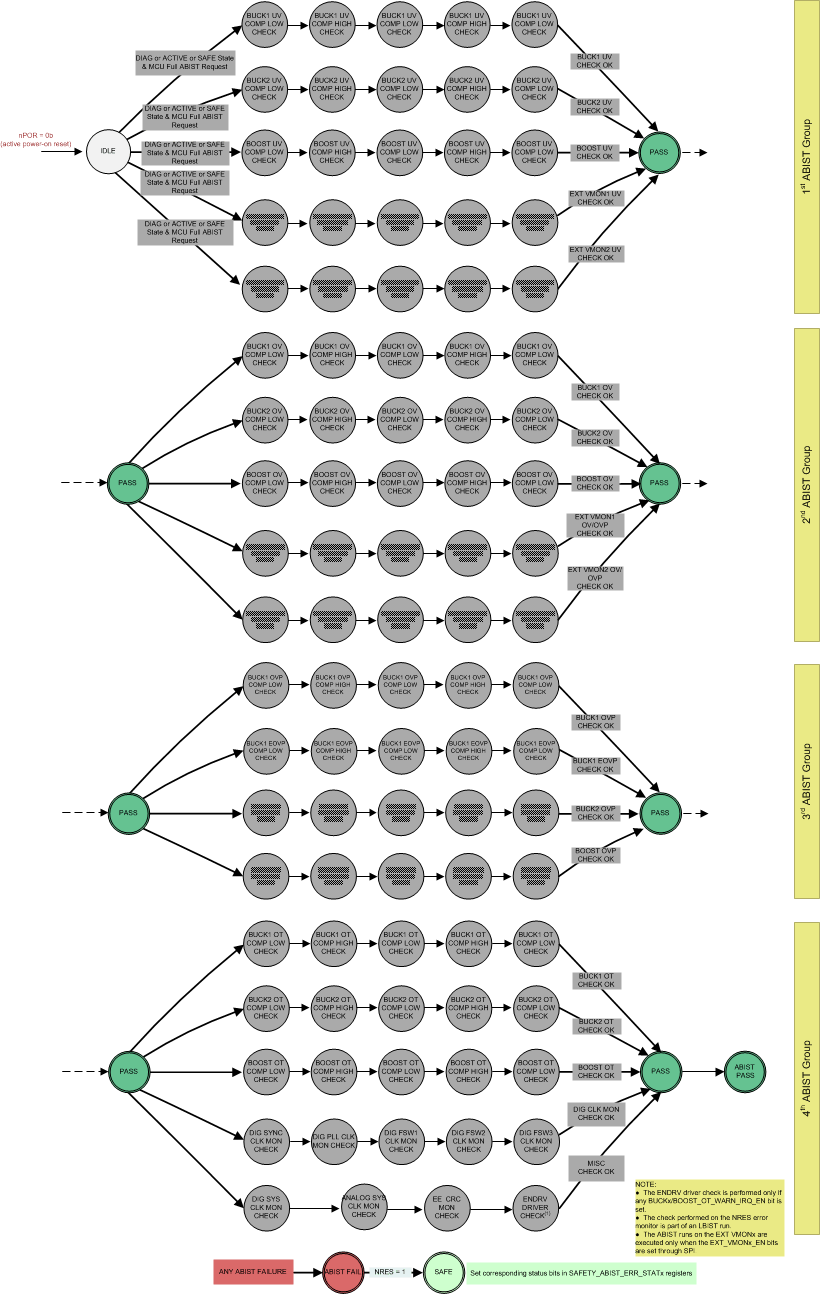
The number of ABIST groups of tests depends on how many ABIST_GROUPx_START bits have been set while the ABIST_SCHED_EN configuration bit in the SAFETY_CFG2 register is not set. The options are four ABIST group of tests (or a full ABIST run), three ABIST group of tests, two ABIST group of tests, or just one ABIST group of tests. Examples of the different groups of tests include any of the following:
- ABIST Group 1 → ABIST Group 2 → ABIST Group 3 → ABIST Group 4, or
- ABIST Group 1 → ABIST Group 2 → ABIST Group 3, or
- ABIST Group 1 → ABIST Group 3 → ABIST Group 4, or
- ABIST Group 2 → ABIST Group 3 → ABIST Group 4, or
- ABIST Group 1 → ABIST Group 2, or
- ABIST Group 1 → ABIST Group 3, or
- ABIST Group 1 → ABIST Group 4, or
- ABIST Group 2 → ABIST Group 3, or
- ABIST Group 2 → ABIST Group 4, or
- ABIST Group 3 → ABIST Group 4, or
- ABIST Group 1, or
- ABIST Group 2, or
- ABIST Group 3, or
- ABIST Group 4
The full ABIST run, when the device is in the DIAGNOSTIC or ACTIVE state, includes a diagnostic check of the error monitor for the ENDRV/nIRQ output driver by allowing comparators in the overtemperature monitors (ABIST Group 4) to toggle the ENDRV/nIRQ pin in a known pattern for the duration of an analog comparator test, if any of the BUCKx/BOOST_OT_WARN_IRQ_EN bits are set. The ABIST of the overtemperature monitors includes both the warning and shutdown comparators. When the device is in the SAFE state, the ENDRV/nIRQ pin is always pulled to logic 0.
The diagnostics of the error monitor for the NRES output driver is performed by the LBIST.
At any time when an ABIST group of tests is set to run, the ABIST tests are activated only during the analog comparator output steady state (sampled analog comparator output matches respective deglitched output and SPI status bit).
If none of these conditions are met, then initiation of an ABIST run is delayed. The maximum wait time of an ABIST start is limited by its ABIST time-out function, which is ≈112 µs.
The full ABIST run is activated by setting all four ABIST_GROUPx_START control bits in the SAFETY_ABIST_CTRL register. As each ABIST group of tests are complete, a corresponding ABIST_GROUPx_DONE status bit is set in the SAFETY_ABIST_ERR_STAT1 status register. This ABIST_GROUPx_DONE status bit is cleared when the corresponding ABIST group of tests are running and is set to 1b when the corresponding ABIST group of tests are complete.
If any of scheduled diagnostic tests fail during an ABIST run or an ABIST time-out occurs and the ABIST_ACTIVE_FAIL_RESP bit is set to 0b, then the following occurs:
- The device goes into the SAFE state.
- One or more ABIST error
status bits in the SAFETY_ABIST_ERR_STAT1 through
the SAFETY_ABIST_ERR_STAT6 registers are set. - The ENDRV/nIRQ pin is asserted low to interrupt the external system MCU.
This enables an interrupting of the external MCU in case of a detected ABIST failure and confirms its root cause by reading the SAFETY_ABIST_ERR_STAT1 through the SAFETY_ABIST_ERR_STAT6 status registers.
If any of the scheduled diagnostic tests fail during an ABIST run or an ABIST time-out occurs, and the ABIST_ACTIVE_FAIL_RESP bit is set to 1b, then the following occurs:
- The device does not change state.
- One or more ABIST error
status bits in the SAFETY_ABIST_ERR_STAT1 through
the SAFETY_ABIST_ERR_STAT6 registers are set.
Undervoltage and overvoltage comparator diagnostic tests do not impact the regulated output-voltage rails. This ABIST run does not include a circuit check of the regulator current-limit, VREG UV and VREG OV, and VIN UV and VIN OV diagnostic checks. When the VREG regulator is enabled, running the VREG UV and VREG OV diagnostics causes the VREG output to become uncontrollable, and for that reason it is excluded from this ABIST run.
 Figure 11-8 ABIST Delayed Test Pulses
In the DIAGNOSTIC and SAFE state, the time interval, t2 (time delay measured from the falling edge of test pulse n and the next rising edge of test pulse n+1), is a couple of system clock cycles.

- ENDRV toggling is checked by the system MCU.
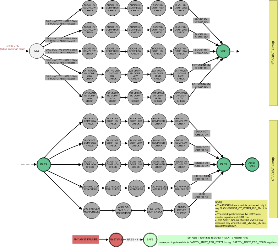
Figure 11-10 shows an example for
running only the tests for the ABIST Group 1 and ABIST Group 4 groups by setting the
ABIST_GROUP1_START and ABIST_GROUP42_START control bits in the
SAFETY_ABIST_CTRL register.

- ENDRV toggling is checked by the system MCU.