ZHCSP40B October 2021 – June 2022 LMX2571-EP
PRODUCTION DATA
- 1 特性
- 2 应用
- 3 说明
- 4 Revision History
- 5 Pin Configuration and Functions
- 6 Specifications
-
7 Detailed Description
- 7.1 Overview
- 7.2 Functional Block Diagram
- 7.3
Feature Description
- 7.3.1 Differences Between the LMX2571 and LMX2571-EP
- 7.3.2 Reference Oscillator Input
- 7.3.3 R-Dividers and Multiplier
- 7.3.4 PLL Phase Detector and Charge Pump
- 7.3.5 PLL N-Divider and Fractional Circuitry
- 7.3.6 Partially Integrated Loop Filter
- 7.3.7 Low-Noise, Fully Integrated VCO
- 7.3.8 External VCO Support
- 7.3.9 Programmable RF Output Divider
- 7.3.10 Programmable RF Output Buffer
- 7.3.11 Integrated TX, RX Switch
- 7.3.12 Power Down
- 7.3.13 Lock Detect
- 7.3.14 FSK Modulation
- 7.3.15 FastLock
- 7.3.16 Register Readback
- 7.4 Device Functional Modes
- 7.5 Programming
- 7.6
Register Maps
- 7.6.1 R60 Register (offset = 3Ch) [reset = 4000h]
- 7.6.2 R58 Register (offset = 3Ah) [reset = C00h]
- 7.6.3 R53 Register (offset = 35h) [reset = 2802h]
- 7.6.4 R47 Register (offset = 2Fh) [reset = 0h]
- 7.6.5 R46 Register (offset = 2Eh) [reset = 1Ah]
- 7.6.6 R42 Register (offset = 2Ah) [reset = 210h]
- 7.6.7 R41 Register (offset = 29h) [reset = 810h]
- 7.6.8 R40 Register (offset = 28h) [reset = 101Ch]
- 7.6.9 R39 Register (offset = 27h) [reset = 11F0h]
- 7.6.10 R35 Register (offset = 23h) [reset = 647h]
- 7.6.11 R34 Register (offset = 22h) [reset = 1000h]
- 7.6.12 R33 Register (offset = 21h) [reset = 0h]
- 7.6.13 R25 to R32 Register (offset = 19h to 20h) [reset = 0h]
- 7.6.14 R24 Register (offset = 18h) [reset = 10h]
- 7.6.15 R23 Register (offset = 17h) [reset = 10A4h]
- 7.6.16 R22 Register (offset = 16h) [reset = 8584h]
- 7.6.17 R21 Register (offset = 15h) [reset = 101h]
- 7.6.18 R20 Register (offset = 14h) [reset = 28h]
- 7.6.19 R19 Register (offset = 13h) [reset = 0h]
- 7.6.20 R18 Register (offset = 12h) [reset = 0h]
- 7.6.21 R17 Register (offset = 11h) [reset = 0h]
- 7.6.22 R9 to R16 Register (offset = 9h to 10h) [reset = 0h]
- 7.6.23 R8 Register (offset = 8h) [reset = 10h]
- 7.6.24 R7 Register (offset = 7h) [reset = 10A4h]
- 7.6.25 R6 Register (offset = 6h) [reset = 8584h]
- 7.6.26 R5 Register (offset = 5h) [reset = 101h]
- 7.6.27 R4 Register (offset = 4h) [reset = 28h]
- 7.6.28 R3 Register (offset = 3h) [reset = 0h]
- 7.6.29 R2 Register (offset = 2h) [reset = 0h]
- 7.6.30 R1 Register (offset = 1h) [reset = 0h]
- 7.6.31 R0 Register (offset = 0h) [reset = 3h]
-
8 Application and Implementation
- 8.1
Application Information
- 8.1.1 Direct Digital FSK Modulation
- 8.1.2 Frequency and Output Port Switching
- 8.1.3 OSCin Configuration
- 8.1.4 Register R0 F1F2_INIT, F1F2_MODE Usage
- 8.1.5 FastLock With External VCO
- 8.1.6 OSCin Slew Rate
- 8.1.7 RF Output Buffer Power Control
- 8.1.8 RF Output Buffer Type
- 8.1.9 MULT Multiplier
- 8.1.10 Integrated VCO
- 8.2 Typical Applications
- 8.3 Do's and Don'ts
- 8.1
Application Information
- 9 Power Supply Recommendations
- 10Layout
- 11Device and Documentation Support
- 12Mechanical, Packaging, and Orderable Information
8.1.1 Direct Digital FSK Modulation
In fractional mode, the finest delta frequency difference between two programmable output frequencies is equal to:
In other words, when the fractional numerator is incremented by 1 (one step), the output frequency will change by Δfmin. A two steps increment will therefore change the frequency by 2 × Δfmin.
In FSK operation, the instantaneous carrier frequency is kept changing among some pre-defined frequencies. In general, the instantaneous carrier frequency is defined as a certain frequency deviation from the nominal carrier frequency. The frequency deviation could be positive and negative.
 Figure 8-1 General FSK Definition
 Figure 8-2 Typical 4FSK Definition
The following equations define the number of steps required for the desired frequency deviation with respect to the nominal carrier frequency output at the RFoutTx or RFoutRx port.
| POLARITY | SYNTHESIZER MODE | PLL MODE |
|---|---|---|
| POSITIVE SWING | Equation 4. 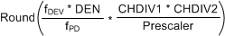 | Equation 5.  |
| NEGATIVE SWING | Equation 6. 2's complement of Equation 4 | Equation 7. 2's complement of Equation 5 |
In FSK PIN mode and FSK SPI mode, register R25-32 and R9-16 are used to store the desired FSK frequency deviations in term of the number of step as defined in the above equations. The order of the registers, 0 to 7, depends on the application system. Figure 8-2 shows a typical 4FSK definition. In this case, FSK_DEV0_Fx and FSK_DEV1_Fx shall be calculated using Equation 4 or Equation 5 while FSK_DEV2_Fx and FSK_DEV3_Fx shall be calculated using Equation 6 or Equation 7.
For example, if FSK PIN mode is enabled in F1 to support 4FSK modulation, set
FSK_MODE_SEL1 = 0
FSK_MODE_SEL0 = 0
FSK_LEVEL = 2
FSK_EN_F1 = 1
| RAW FSK DATA STREAM INPUT | EQUIVALENT SYMBOL INPUT | REGISTER SELECTED | RF OUTPUT |
|---|---|---|---|
 | 10 | FSK_DEV2_F1 | 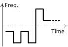 |
| 11 | FSK_DEV3_F1 | ||
| 10 | FSK_DEV2_F1 | ||
| 11 | FSK_DEV3_F1 | ||
| 01 | FSK_DEV1_F1 | ||
| 00 | FSK_DEV0_F1 | ||
| ... | ... |
FSK SPI mode assumes the user knows which symbol to send; user can directly write to register R34, FSK_DEV_SEL to select the desired frequency deviation.
For example, to enable the device to support 4FSK modulation at F1 using FSK SPI mode, set
FSK_MODE_SEL1 = 0
FSK_MODE_SEL0 = 1
FSK_LEVEL = 2
FSK_EN_F1 = 1
| DESIRED SYMBOL | WRITE REGISTER FSK_DEV_SEL | REGISTER SELECTED |
|---|---|---|
| 10 | 2 | FSK_DEV2_F1 |
| 11 | 3 | FSK_DEV3_F1 |
| 10 | 2 | FSK_DEV2_F1 |
| 11 | 3 | FSK_DEV3_F1 |
| 01 | 1 | FSK_DEV1_F1 |
| 00 | 0 | FSK_DEV0_F1 |
| ... | ... | … |
Both the FSK PIN mode and FSK SPI mode support up to 8 levels of FSK. To support an arbitrary-level FSK, use FSK SPI FAST mode or FSK I2S mode. Constructing pulse-shaping FSK modulation by over-sampling the FSK modulation waveform is one of the use cases of these modes.
Analog-FM modulation can also be produced in these modes. For example, with a 1-kHz sine wave modulation signal with peak frequency deviation of ±2 kHz, the signal can be over-sampled, say 10 times. Each sample point corresponding to a scaled frequency deviation.
 Figure 8-3 Over-Sampling Modulation Signal
In FSK SPI FAST mode, write the desired FSK steps directly to register R33, FSK_DEV_SPI_FAST. To enable this mode, set
FSK_MODE_SEL1 = 1
FSK_MODE_SEL0 = 1
FSK_EN_F1 = 1
| TIME | FREQUENCY DEVIATION | CORRESPONDING FSK STEPS(1) | BINARY EQUIVALENT | WRITE TO FSK_DEV_SPI_FAST |
|---|---|---|---|---|
| t0 | 618.034 Hz | 518 | 0000 0010 0000 0110 | 518 |
| t1 | 1618.034 Hz | 1357 | 0000 0101 0100 1101 | 1357 |
| t2 | 2000 Hz | 1678 | 0000 0110 1000 1110 | 1678 |
| … | … | … | … | … |
| t6 | –1618.034 Hz | 64178 | 1111 1010 1011 0010 | 64178 |
| t7 | –2000 Hz | 63857 | 1111 1001 0111 0001 | 63857 |
| … | … | … | … | … |
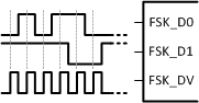
In FSK I2S mode, clock in the desired binary format FSK steps in the FSK_D1 pin.
 Figure 8-4 FSK I2S Mode Example
To enable FSK I2S mode, set
FSK_MODE_SEL1 = 1
FSK_MODE_SEL0 = 0
FSK_EN_F1 =1