ZHCSP40B October 2021 – June 2022 LMX2571-EP
PRODUCTION DATA
- 1 特性
- 2 应用
- 3 说明
- 4 Revision History
- 5 Pin Configuration and Functions
- 6 Specifications
-
7 Detailed Description
- 7.1 Overview
- 7.2 Functional Block Diagram
- 7.3
Feature Description
- 7.3.1 Differences Between the LMX2571 and LMX2571-EP
- 7.3.2 Reference Oscillator Input
- 7.3.3 R-Dividers and Multiplier
- 7.3.4 PLL Phase Detector and Charge Pump
- 7.3.5 PLL N-Divider and Fractional Circuitry
- 7.3.6 Partially Integrated Loop Filter
- 7.3.7 Low-Noise, Fully Integrated VCO
- 7.3.8 External VCO Support
- 7.3.9 Programmable RF Output Divider
- 7.3.10 Programmable RF Output Buffer
- 7.3.11 Integrated TX, RX Switch
- 7.3.12 Power Down
- 7.3.13 Lock Detect
- 7.3.14 FSK Modulation
- 7.3.15 FastLock
- 7.3.16 Register Readback
- 7.4 Device Functional Modes
- 7.5 Programming
- 7.6
Register Maps
- 7.6.1 R60 Register (offset = 3Ch) [reset = 4000h]
- 7.6.2 R58 Register (offset = 3Ah) [reset = C00h]
- 7.6.3 R53 Register (offset = 35h) [reset = 2802h]
- 7.6.4 R47 Register (offset = 2Fh) [reset = 0h]
- 7.6.5 R46 Register (offset = 2Eh) [reset = 1Ah]
- 7.6.6 R42 Register (offset = 2Ah) [reset = 210h]
- 7.6.7 R41 Register (offset = 29h) [reset = 810h]
- 7.6.8 R40 Register (offset = 28h) [reset = 101Ch]
- 7.6.9 R39 Register (offset = 27h) [reset = 11F0h]
- 7.6.10 R35 Register (offset = 23h) [reset = 647h]
- 7.6.11 R34 Register (offset = 22h) [reset = 1000h]
- 7.6.12 R33 Register (offset = 21h) [reset = 0h]
- 7.6.13 R25 to R32 Register (offset = 19h to 20h) [reset = 0h]
- 7.6.14 R24 Register (offset = 18h) [reset = 10h]
- 7.6.15 R23 Register (offset = 17h) [reset = 10A4h]
- 7.6.16 R22 Register (offset = 16h) [reset = 8584h]
- 7.6.17 R21 Register (offset = 15h) [reset = 101h]
- 7.6.18 R20 Register (offset = 14h) [reset = 28h]
- 7.6.19 R19 Register (offset = 13h) [reset = 0h]
- 7.6.20 R18 Register (offset = 12h) [reset = 0h]
- 7.6.21 R17 Register (offset = 11h) [reset = 0h]
- 7.6.22 R9 to R16 Register (offset = 9h to 10h) [reset = 0h]
- 7.6.23 R8 Register (offset = 8h) [reset = 10h]
- 7.6.24 R7 Register (offset = 7h) [reset = 10A4h]
- 7.6.25 R6 Register (offset = 6h) [reset = 8584h]
- 7.6.26 R5 Register (offset = 5h) [reset = 101h]
- 7.6.27 R4 Register (offset = 4h) [reset = 28h]
- 7.6.28 R3 Register (offset = 3h) [reset = 0h]
- 7.6.29 R2 Register (offset = 2h) [reset = 0h]
- 7.6.30 R1 Register (offset = 1h) [reset = 0h]
- 7.6.31 R0 Register (offset = 0h) [reset = 3h]
-
8 Application and Implementation
- 8.1
Application Information
- 8.1.1 Direct Digital FSK Modulation
- 8.1.2 Frequency and Output Port Switching
- 8.1.3 OSCin Configuration
- 8.1.4 Register R0 F1F2_INIT, F1F2_MODE Usage
- 8.1.5 FastLock With External VCO
- 8.1.6 OSCin Slew Rate
- 8.1.7 RF Output Buffer Power Control
- 8.1.8 RF Output Buffer Type
- 8.1.9 MULT Multiplier
- 8.1.10 Integrated VCO
- 8.2 Typical Applications
- 8.3 Do's and Don'ts
- 8.1
Application Information
- 9 Power Supply Recommendations
- 10Layout
- 11Device and Documentation Support
- 12Mechanical, Packaging, and Orderable Information
8.1.6 OSCin Slew Rate
A phase-lock loop consists of a clean reference clock, a PLL, and a VCO. Each of these contributes to the total phase noise. The LMX2571-EP is a high-performance PLL with integrated VCO. Both PLL noise and VCO noise are very good. Typical PLL 1/f noise and noise floor are –124 dBc/Hz and –231 dBc/Hz, respectively. To get the best possible phase-noise performance from the device the quality of the reference clock is very important because it may add noise to the loop. First of all, the phase noise of the reference clock must be good so that the final performance of the system is not degraded. Furthermore, using reference clock with a rather high slew rate (such as a square wave) is highly preferred. Driving the device input with a lower slew rate clock will degrade the device phase noise.
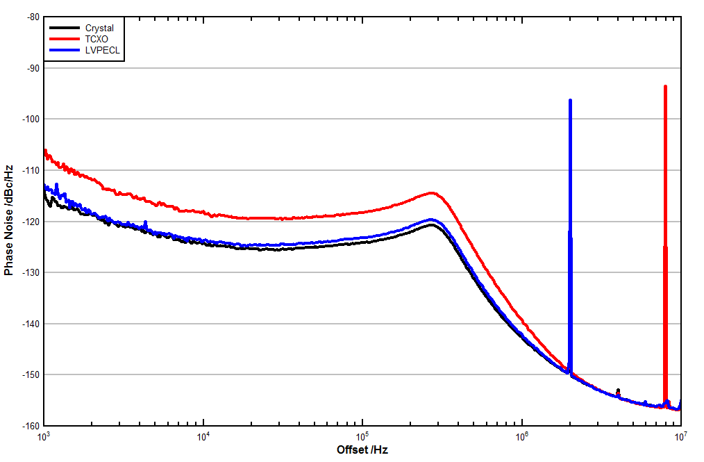
For a given frequency, a sine wave clock has the slowest slew rate, especially when the frequency is low. A CMOS clock or differential clock have much faster slew rates and are recommended. Figure 8-10 shows a phase-noise comparison with different types of reference clocks. Output frequency is 480 MHz while the input clock frequency is 26 MHz. As one can see, there is a 5-dB difference in phase noise when using a clipped sine wave TCXO compared to a differential LVPECL clock. Note that the crystal option is not available in the LMX2571-EP, but is included in the LMX2571 for comparison purposes.
 Figure 8-10 Phase Noise vs. Input Clock