ZHCSPK7F November 2004 – January 2022 TPS2384
PRODUCTION DATA
- 1 特性
- 2 应用
- 3 说明
- 4 Revision History
- 5 Pin Configuration and Functions
- 6 Specifications
- 7 Parameter Measurement Information
-
8 Detailed Description
- 8.1 Overview
- 8.2 Functional Block Diagrams
- 8.3 Feature Description
- 8.4
Device Functional Modes
- 8.4.1 Auto Mode
- 8.4.2 Auto Mode Functional Description
- 8.4.3 AM Faults and INTB Output
- 8.4.4 Over and Undervoltage Fault
- 8.4.5 Over Current or Current Limit Faults
- 8.4.6 Undercurrent Fault (DC Modulated Disconnect)
- 8.4.7 Power Management Mode (PMM)
- 8.4.8 PMM Discovery 1
- 8.4.9 PMM Discovery 2
- 8.4.10 PMM Classification
- 8.4.11 PMM Legacy
- 8.4.12 PMM Rup Pwr
- 8.4.13 PMM RDWN
- 8.5 Programming
- 8.6
Register Maps
- 8.6.1 Register/Port Addressing Map
- 8.6.2 Common Read, Register Select
- 8.6.3 Common Write, Register Select = 1111 (Test Register)
- 8.6.4 Common Control Write, Register Select = 0001
- 8.6.5 Port Control Write 1, Register Select = 0010 (One Per Port)
- 8.6.6 Port Control Write 2, Register Select = 0011 (One Per Port)
- 8.6.7 Port Status Read 1, Register Select = 0100 (One Per Port)
- 8.6.8 Port Status Read 2, Register Select = 0101 (One Per Port)
- 8.6.9
A/D Results Registers (Discovery Current, Voltage, Current and Temperature)
- 8.6.9.1 Discovery Current — Lower Bits, Register Select = 0110 (One Per Port)
- 8.6.9.2 Discovery Current — Upper Bits, Register Select = 0111 (One Per Port)
- 8.6.9.3 Voltage — Lower Bits, Register Select = 1000 (One Per Port)
- 8.6.9.4 Voltage — Upper Bits, Register Select = 1001 (One Per Port)
- 8.6.9.5 Current — Lower Bits, Register Select = 1010 (One Per Port)
- 8.6.9.6 Current — Upper Bits, Register Select = 1011 (One Per Port)
- 8.6.9.7 Temperature — Lower Bits, Register Select = 1100 (One Per Port)
- 8.6.9.8 Temperature — Upper Bits, Register Select = 1101 (One Per Port)
- 9 Application and Implementation
- 10Power Supply Recommendations
- 11Layout
- 12Device and Documentation Support
- 13Mechanical, Packaging, and Orderable Information
封装选项
机械数据 (封装 | 引脚)
散热焊盘机械数据 (封装 | 引脚)
订购信息
8.4.2.2 AM Classification
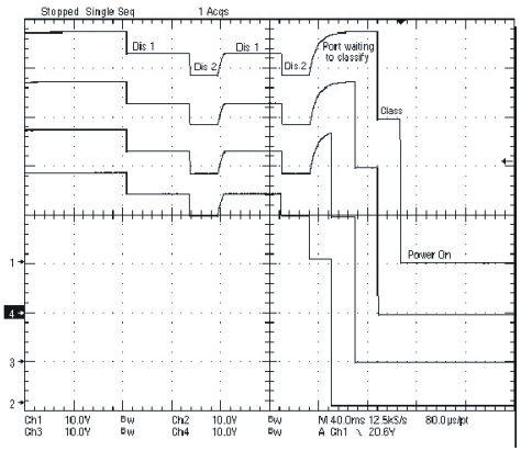
After a successful discovery of a valid PD, the TPS2384 enters the classification function that identifies the power level based on the PD's current signature. The classification current level is measured at a reduced terminal voltage of 17.5 V. During classification the power dissipation can be at its highest; therefore, to prevent overtemperature shutdown in auto mode, only one port classifies at a time. When multiple ports successfully discover and proceed to classification at the same time the auto sequencer processes each request separately allowing only one port to enter classification. Figure 8-5 shows all four ports successfully detecting a valid PD at the same time and then the classification of each port occurring separately.
 Figure 8-5 Four Port Discovery, Class, Power On
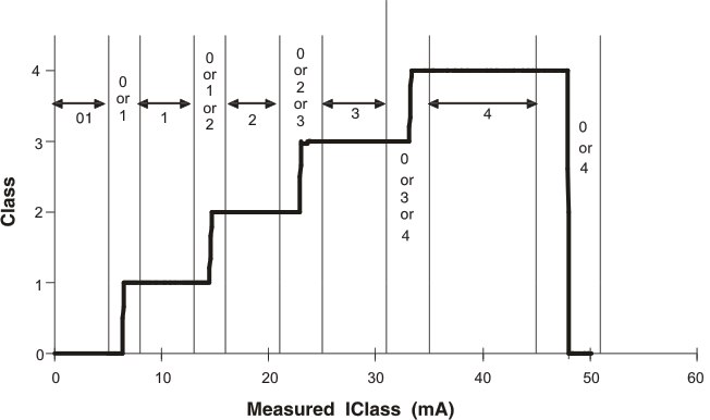
Upon completion of classification, the port classification register is updated. In AM mode, this information is not used but for semi-auto mode the class information can be used for power management. Figure 8-6 shows actual class currents and the class assignment which were stored in the register. These assignments are compliant with the IEEE 802.3af Standard
 Figure 8-6 Class Current and Class Assignments