ZHCSHE0 December 2017 TMS320F28377D-EP
PRODUCTION DATA.
- 1器件概述
- 2Revision History
- 3Terminal Configuration and Functions
-
4Specifications
- 4.1 Absolute Maximum Ratings
- 4.2 ESD Ratings
- 4.3 Recommended Operating Conditions
- 4.4 Power Consumption Summary
- 4.5 Electrical Characteristics
- 4.6 Thermal Resistance Characteristics
- 4.7
System
- 4.7.1 Power Sequencing
- 4.7.2 Reset Timing
- 4.7.3
Clock Specifications
- 4.7.3.1 Clock Sources
- 4.7.3.2 Clock Frequencies, Requirements, and Characteristics
- 4.7.3.3 Input Clocks and PLLs
- 4.7.3.4 Crystal Oscillator
- 4.7.3.5 Internal Oscillators
- 4.7.4 Flash Parameters
- 4.7.5 Emulation/JTAG
- 4.7.6 GPIO Electrical Data and Timing
- 4.7.7 Interrupts
- 4.7.8
Low-Power Modes
- 4.7.8.1 Clock-Gating Low-Power Modes
- 4.7.8.2 Power-Gating Low-Power Modes
- 4.7.8.3
Low-Power Mode Wakeup Timing
- Table 4-29 IDLE Mode Timing Requirements
- Table 4-30 IDLE Mode Switching Characteristics
- Table 4-31 STANDBY Mode Timing Requirements
- Table 4-32 STANDBY Mode Switching Characteristics
- Table 4-33 HALT Mode Timing Requirements
- Table 4-34 HALT Mode Switching Characteristics
- Table 4-35 HIBERNATE Mode Timing Requirements
- Table 4-36 HIBERNATE Mode Switching Characteristics
- 4.7.9 External Memory Interface (EMIF)
- 4.8
Analog Peripherals
- 4.8.1
Analog-to-Digital Converter (ADC)
- 4.8.1.1
ADC Electrical Data and Timing
- Table 4-41 ADC Operating Conditions (16-Bit Differential Mode)
- Table 4-42 ADC Characteristics (16-Bit Differential Mode)
- Table 4-43 ADC Operating Conditions (12-Bit Single-Ended Mode)
- Table 4-44 ADC Characteristics (12-Bit Single-Ended Mode)
- Table 4-45 ADCEXTSOC Timing Requirements
- 4.8.1.1.1 ADC Input Models
- 4.8.1.1.2 ADC Timing Diagrams
- 4.8.1.2 Temperature Sensor Electrical Data and Timing
- 4.8.1.1
ADC Electrical Data and Timing
- 4.8.2 Comparator Subsystem (CMPSS)
- 4.8.3 Buffered Digital-to-Analog Converter (DAC)
- 4.8.1
Analog-to-Digital Converter (ADC)
- 4.9
Control Peripherals
- 4.9.1 Enhanced Capture (eCAP)
- 4.9.2 Enhanced Pulse Width Modulator (ePWM)
- 4.9.3 Enhanced Quadrature Encoder Pulse (eQEP)
- 4.9.4 High-Resolution Pulse Width Modulator (HRPWM)
- 4.9.5 Sigma-Delta Filter Module (SDFM)
- 4.10
Communications Peripherals
- 4.10.1 Controller Area Network (CAN)
- 4.10.2 Inter-Integrated Circuit (I2C)
- 4.10.3
Multichannel Buffered Serial Port (McBSP)
- 4.10.3.1
McBSP Electrical Data and Timing
- 4.10.3.1.1 McBSP Transmit and Receive Timing
- 4.10.3.1.2
McBSP as SPI Master or Slave Timing
- Table 4-69 McBSP as SPI Master or Slave Timing Requirements (CLKSTP = 10b, CLKXP = 0)
- Table 4-70 McBSP as SPI Master or Slave Switching Characteristics (CLKSTP = 10b, CLKXP = 0)
- Table 4-71 McBSP as SPI Master or Slave Timing Requirements (CLKSTP = 11b, CLKXP = 0)
- Table 4-72 McBSP as SPI Master or Slave Switching Characteristics (CLKSTP = 11b, CLKXP = 0)
- Table 4-73 McBSP as SPI Master or Slave Timing Requirements (CLKSTP = 10b, CLKXP = 1)
- Table 4-74 McBSP as SPI Master or Slave Switching Characteristics (CLKSTP = 10b, CLKXP = 1)
- Table 4-75 McBSP as SPI Master or Slave Timing Requirements (CLKSTP = 11b, CLKXP = 1)
- Table 4-76 McBSP as SPI Master or Slave Switching Characteristics (CLKSTP = 11b, CLKXP = 1)
- 4.10.3.1
McBSP Electrical Data and Timing
- 4.10.4 Serial Communications Interface (SCI)
- 4.10.5 Serial Peripheral Interface (SPI)
- 4.10.6 Universal Serial Bus (USB) Controller
- 4.10.7 Universal Parallel Port (uPP) Interface
-
5Detailed Description
- 5.1 Overview
- 5.2 Functional Block Diagram
- 5.3 Memory
- 5.4 Identification
- 5.5 Bus Architecture – Peripheral Connectivity
- 5.6 C28x Processor
- 5.7 Control Law Accelerator
- 5.8 Direct Memory Access
- 5.9 Interprocessor Communication Module
- 5.10 Boot ROM and Peripheral Booting
- 5.11 Dual Code Security Module
- 5.12 Timers
- 5.13 Nonmaskable Interrupt With Watchdog Timer (NMIWD)
- 5.14 Watchdog
- 5.15 Configurable Logic Block (CLB)
- 6Applications, Implementation, and Layout
- 7器件和文档支持
- 8机械封装和可订购信息
封装选项
机械数据 (封装 | 引脚)
散热焊盘机械数据 (封装 | 引脚)
- PTP|176
订购信息
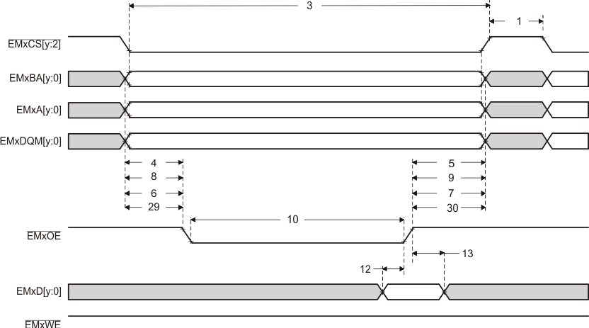
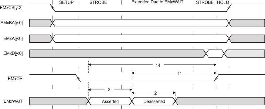
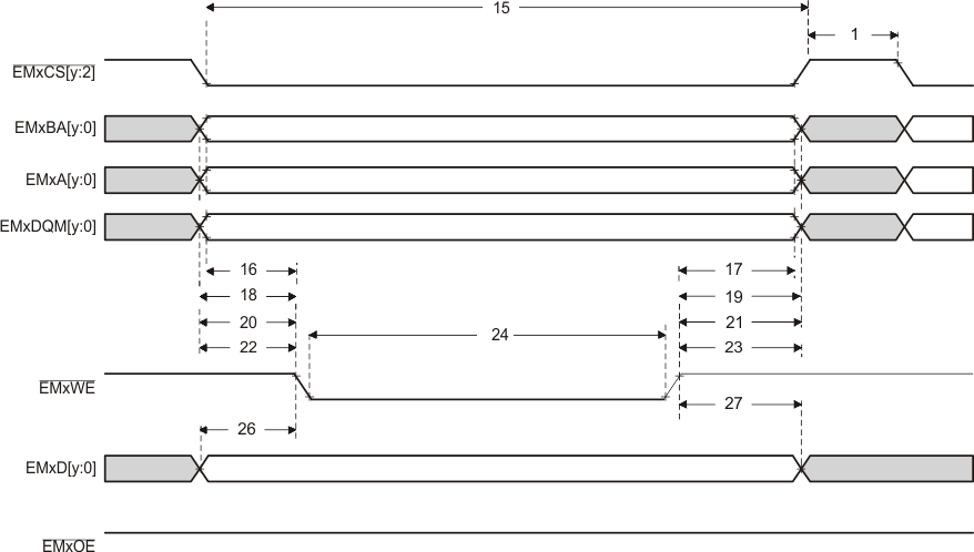
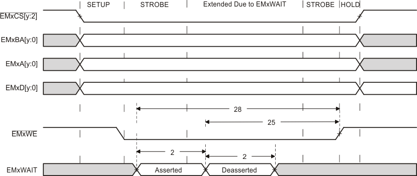
Table 4-38 EMIF Asynchronous Memory Switching Characteristics(1)(2)(3)
| NO. | PARAMETER | MIN | MAX | UNIT | |
|---|---|---|---|---|---|
| Reads and Writes | |||||
| 1 | td(TURNAROUND) | Turn around time | (TA)*E–3 | (TA)*E+2 | ns |
| Reads | |||||
| 3 | tc(EMRCYCLE) | EMIF read cycle time (EW = 0) | (RS+RST+RH+2)*E–3 | (RS+RST+RH+2)*E+2 | ns |
| EMIF read cycle time (EW = 1) | (RS+RST+RH+2+ (EWC*16))*E–3 |
(RS+RST+RH+2+ (EWC*16))*E+2 |
ns | ||
| 4 | tsu(EMCEL-EMOEL) | Output setup time, EMxCS[y:2] low to EMxOE low (SS = 0) | (RS)*E–3 | (RS)*E+2 | ns |
| Output setup time, EMxCS[y:2] low to EMxOE low (SS = 1) | –3 | 2 | ns | ||
| 5 | th(EMOEH-EMCEH) | Output hold time, EMxOE high to EMxCS[y:2] high (SS = 0) | (RH)*E–3 | (RH)*E | ns |
| Output hold time, EMxOE high to EMxCS[y:2] high (SS = 1) | –3 | 0 | ns | ||
| 6 | tsu(EMBAV-EMOEL) | Output setup time, EMxBA[y:0] valid to EMxOE low | (RS)*E–3 | (RS)*E+2 | ns |
| 7 | th(EMOEH-EMBAIV) | Output hold time, EMxOE high to EMxBA[y:0] invalid | (RH)*E–3 | (RH)*E | ns |
| 8 | tsu(EMAV-EMOEL) | Output setup time, EMxA[y:0] valid to EMxOE low | (RS)*E–3 | (RS)*E+2 | ns |
| 9 | th(EMOEH-EMAIV) | Output hold time, EMxOE high to EMxA[y:0] invalid | (RH)*E–3 | (RH)*E | ns |
| 10 | tw(EMOEL) | EMxOE active low width (EW = 0) | (RST)*E–1 | (RST)*E+1 | ns |
| EMxOE active low width (EW = 1) | (RST+(EWC*16))*E–1 | (RST+(EWC*16))*E+1 | ns | ||
| 11 | td(EMWAITH-EMOEH) | Delay time from EMxWAIT deasserted to EMxOE high | 4E+10 | 5E+15 | ns |
| 29 | tsu(EMDQMV-EMOEL) | Output setup time, EMxDQM[y:0] valid to EMxOE low | (RS)*E–3 | (RS)*E+2 | ns |
| 30 | th(EMOEH-EMDQMIV) | Output hold time, EMxOE high to EMxDQM[y:0] invalid | (RH)*E–3 | (RH)*E | ns |
| Writes | |||||
| 15 | tc(EMWCYCLE) | EMIF write cycle time (EW = 0) | (WS+WST+WH+2)*E–3 | (WS+WST+WH+2)*E+1 | ns |
| EMIF write cycle time (EW = 1) | (WS+WST+WH+2+ (EWC*16))*E–3 |
(WS+WST+WH+2+ (EWC*16))*E+1 |
ns | ||
| 16 | tsu(EMCEL-EMWEL) | Output setup time, EMxCS[y:2] low to EMxWE low (SS = 0) | (WS)*E–3 | (WS)*E+1 | ns |
| Output setup time, EMxCS[y:2] low to EMxWE low (SS = 1) | –3 | 1 | ns | ||
| 17 | th(EMWEH-EMCEH) | Output hold time, EMxWE high to EMxCS[y:2] high (SS = 0) | (WH)*E–3 | (WH)*E | ns |
| Output hold time, EMxWE high to EMxCS[y:2] high (SS = 1) | –3 | 0 | ns | ||
| 18 | tsu(EMDQMV-EMWEL) | Output setup time, EMxDQM[y:0] valid to EMxWE low | (WS)*E–3 | (WS)*E+1 | ns |
| 19 | th(EMWEH-EMDQMIV) | Output hold time, EMxWE high to EMxDQM[y:0] invalid | (WH)*E–3 | (WH)*E | ns |
| 20 | tsu(EMBAV-EMWEL) | Output setup time, EMxBA[y:0] valid to EMxWE low | (WS)*E–3 | (WS)*E+1 | ns |
| 21 | th(EMWEH-EMBAIV) | Output hold time, EMxWE high to EMxBA[y:0] invalid | (WH)*E–3 | (WH)*E | ns |
| 22 | tsu(EMAV-EMWEL) | Output setup time, EMxA[y:0] valid to EMxWE low | (WS)*E–3 | (WS)*E+1 | ns |
| 23 | th(EMWEH-EMAIV) | Output hold time, EMxWE high to EMxA[y:0] invalid | (WH)*E–3 | (WH)*E | ns |
| 24 | tw(EMWEL) | EMxWE active low width (EW = 0) |
(WST)*E–1 | (WST)*E+1 | ns |
| EMxWE active low width (EW = 1) |
(WST+(EWC*16))*E–1 | (WST+(EWC*16))*E+1 | ns | ||
| 25 | td(EMWAITH-EMWEH) | Delay time from EMxWAIT deasserted to EMxWE high | 4E+10 | 5E+15 | ns |
| 26 | tsu(EMDV-EMWEL) | Output setup time, EMxD[y:0] valid to EMxWE low | (WS)*E–3 | (WS)*E+1 | ns |
| 27 | th(EMWEH-EMDIV) | Output hold time, EMxWE high to EMxD[y:0] invalid | (WH)*E–3 | (WH)*E | ns |
(1) TA = Turn around, RS = Read setup, RST = Read strobe, RH = Read hold, WS = Write setup, WST = Write strobe, WH = Write hold, MEWC = Maximum external wait cycles. These parameters are programmed through the Asynchronous Bank and Asynchronous Wait Cycle Configuration Registers. These support the following ranges of values: TA[4–1], RS[16–1], RST[64–4], RH[8–1], WS[16–1], WST[64–1], WH[8–1], and MEWC[1–256]. See the TMS320F2837xD Dual-Core Delfino Microcontrollers Technical Reference Manual for more information.
(2) E = EMxCLK period in ns.
(3) EWC = external wait cycles determined by EMxWAIT input signal. EWC supports the following range of values. EWC[256–1]. The maximum wait time before time-out is specified by bit field MEWC in the Asynchronous Wait Cycle Configuration Register. See the TMS320F2837xD Dual-Core Delfino Microcontrollers Technical Reference Manual for more information.
 Figure 4-22 Asynchronous Memory Read Timing
 Figure 4-23 EMxWAIT Read Timing Requirements
 Figure 4-24 Asynchronous Memory Write Timing
 Figure 4-25 EMxWAIT Write Timing Requirements