ZHCSHE0 December 2017 TMS320F28377D-EP
PRODUCTION DATA.
- 1器件概述
- 2Revision History
- 3Terminal Configuration and Functions
-
4Specifications
- 4.1 Absolute Maximum Ratings
- 4.2 ESD Ratings
- 4.3 Recommended Operating Conditions
- 4.4 Power Consumption Summary
- 4.5 Electrical Characteristics
- 4.6 Thermal Resistance Characteristics
- 4.7
System
- 4.7.1 Power Sequencing
- 4.7.2 Reset Timing
- 4.7.3
Clock Specifications
- 4.7.3.1 Clock Sources
- 4.7.3.2 Clock Frequencies, Requirements, and Characteristics
- 4.7.3.3 Input Clocks and PLLs
- 4.7.3.4 Crystal Oscillator
- 4.7.3.5 Internal Oscillators
- 4.7.4 Flash Parameters
- 4.7.5 Emulation/JTAG
- 4.7.6 GPIO Electrical Data and Timing
- 4.7.7 Interrupts
- 4.7.8
Low-Power Modes
- 4.7.8.1 Clock-Gating Low-Power Modes
- 4.7.8.2 Power-Gating Low-Power Modes
- 4.7.8.3
Low-Power Mode Wakeup Timing
- Table 4-29 IDLE Mode Timing Requirements
- Table 4-30 IDLE Mode Switching Characteristics
- Table 4-31 STANDBY Mode Timing Requirements
- Table 4-32 STANDBY Mode Switching Characteristics
- Table 4-33 HALT Mode Timing Requirements
- Table 4-34 HALT Mode Switching Characteristics
- Table 4-35 HIBERNATE Mode Timing Requirements
- Table 4-36 HIBERNATE Mode Switching Characteristics
- 4.7.9 External Memory Interface (EMIF)
- 4.8
Analog Peripherals
- 4.8.1
Analog-to-Digital Converter (ADC)
- 4.8.1.1
ADC Electrical Data and Timing
- Table 4-41 ADC Operating Conditions (16-Bit Differential Mode)
- Table 4-42 ADC Characteristics (16-Bit Differential Mode)
- Table 4-43 ADC Operating Conditions (12-Bit Single-Ended Mode)
- Table 4-44 ADC Characteristics (12-Bit Single-Ended Mode)
- Table 4-45 ADCEXTSOC Timing Requirements
- 4.8.1.1.1 ADC Input Models
- 4.8.1.1.2 ADC Timing Diagrams
- 4.8.1.2 Temperature Sensor Electrical Data and Timing
- 4.8.1.1
ADC Electrical Data and Timing
- 4.8.2 Comparator Subsystem (CMPSS)
- 4.8.3 Buffered Digital-to-Analog Converter (DAC)
- 4.8.1
Analog-to-Digital Converter (ADC)
- 4.9
Control Peripherals
- 4.9.1 Enhanced Capture (eCAP)
- 4.9.2 Enhanced Pulse Width Modulator (ePWM)
- 4.9.3 Enhanced Quadrature Encoder Pulse (eQEP)
- 4.9.4 High-Resolution Pulse Width Modulator (HRPWM)
- 4.9.5 Sigma-Delta Filter Module (SDFM)
- 4.10
Communications Peripherals
- 4.10.1 Controller Area Network (CAN)
- 4.10.2 Inter-Integrated Circuit (I2C)
- 4.10.3
Multichannel Buffered Serial Port (McBSP)
- 4.10.3.1
McBSP Electrical Data and Timing
- 4.10.3.1.1 McBSP Transmit and Receive Timing
- 4.10.3.1.2
McBSP as SPI Master or Slave Timing
- Table 4-69 McBSP as SPI Master or Slave Timing Requirements (CLKSTP = 10b, CLKXP = 0)
- Table 4-70 McBSP as SPI Master or Slave Switching Characteristics (CLKSTP = 10b, CLKXP = 0)
- Table 4-71 McBSP as SPI Master or Slave Timing Requirements (CLKSTP = 11b, CLKXP = 0)
- Table 4-72 McBSP as SPI Master or Slave Switching Characteristics (CLKSTP = 11b, CLKXP = 0)
- Table 4-73 McBSP as SPI Master or Slave Timing Requirements (CLKSTP = 10b, CLKXP = 1)
- Table 4-74 McBSP as SPI Master or Slave Switching Characteristics (CLKSTP = 10b, CLKXP = 1)
- Table 4-75 McBSP as SPI Master or Slave Timing Requirements (CLKSTP = 11b, CLKXP = 1)
- Table 4-76 McBSP as SPI Master or Slave Switching Characteristics (CLKSTP = 11b, CLKXP = 1)
- 4.10.3.1
McBSP Electrical Data and Timing
- 4.10.4 Serial Communications Interface (SCI)
- 4.10.5 Serial Peripheral Interface (SPI)
- 4.10.6 Universal Serial Bus (USB) Controller
- 4.10.7 Universal Parallel Port (uPP) Interface
-
5Detailed Description
- 5.1 Overview
- 5.2 Functional Block Diagram
- 5.3 Memory
- 5.4 Identification
- 5.5 Bus Architecture – Peripheral Connectivity
- 5.6 C28x Processor
- 5.7 Control Law Accelerator
- 5.8 Direct Memory Access
- 5.9 Interprocessor Communication Module
- 5.10 Boot ROM and Peripheral Booting
- 5.11 Dual Code Security Module
- 5.12 Timers
- 5.13 Nonmaskable Interrupt With Watchdog Timer (NMIWD)
- 5.14 Watchdog
- 5.15 Configurable Logic Block (CLB)
- 6Applications, Implementation, and Layout
- 7器件和文档支持
- 8机械封装和可订购信息
封装选项
机械数据 (封装 | 引脚)
散热焊盘机械数据 (封装 | 引脚)
- PTP|176
订购信息
Table 4-54 Buffered DAC Electrical Characteristics
over recommended operating conditions (unless otherwise noted)(1)| PARAMETER | TEST CONDITIONS | MIN | TYP | MAX | UNIT |
|---|---|---|---|---|---|
| Power-up time (DACOUTEN to DAC output valid) | 10 | µs | |||
| Trimmed offset error | Midpoint | –10 | 10 | mV | |
| Gain error(2) | –2.5 | 2.5 | % of FSR | ||
| DNL(3) | Endpoint corrected | > –1 | 1 | LSB | |
| INL | Endpoint corrected | –5 | 5 | LSB | |
| DACOUTx settling time | Settling to 2 LSBs after 0.3V-to-3V transition | 2 | µs | ||
| Resolution | 12 | bits | |||
| Voltage output range(4) | 0.3 | VDDA – 0.3 | V | ||
| Capacitive load | Output drive capability | 100 | pF | ||
| Resistive load | Output drive capability | 5 | kΩ | ||
| RPD | 50 | kΩ | |||
| Reference voltage(5) | VDAC or VREFHI | 2.4 | 2.5 or 3.0 | VDDA | V |
| Reference load(6) | VDAC or VREFHI | 170 | kΩ | ||
| Output noise | Integrated noise from 100 Hz to 100 kHz | 500 | µVrms | ||
| Noise density at 10 kHz | 711 | nVrms/√Hz | |||
| Glitch energy | 1.5 | V-ns | |||
| PSRR(7) | DC up to 1 kHz | 70 | dB | ||
| 100 kHz | 30 | ||||
| SNR | 1020 Hz | 67 | dB | ||
| THD | 1020 Hz | –63 | dB | ||
| SFDR | 1020 Hz, including harmonics and spurs | 66 | dBc | ||
| 1020 Hz, including only spurs | 104 |
(1) Typical values are measured with VREFHI = 3.3 V and VREFLO = 0 V unless otherwise noted. Minimum and Maximum values are tested or characterized with VREFHI = 2.5 V and VREFLO = 0 V.
(2) Gain error is calculated for linear output range.
(3) The DAC output is monotonic.
(4) This is the linear output range of the DAC. The DAC can generate voltages outside this range, but the output voltage will not be linear due to the buffer.
(5) For best PSRR performance, VDAC or VREFHI should be less than VDDA.
(6) Per active Buffered DAC module.
(7) VREFHI = 3.2 V, VDDA = 3.3 V DC + 100 mV Sine.
NOTE
The VDAC pin must be kept below VDDA + 0.3 V to ensure proper functional operation. If the VDAC pin exceeds this level, a blocking circuit may activate, and the internal value of VDAC may float to 0 V internally, giving improper DAC output.
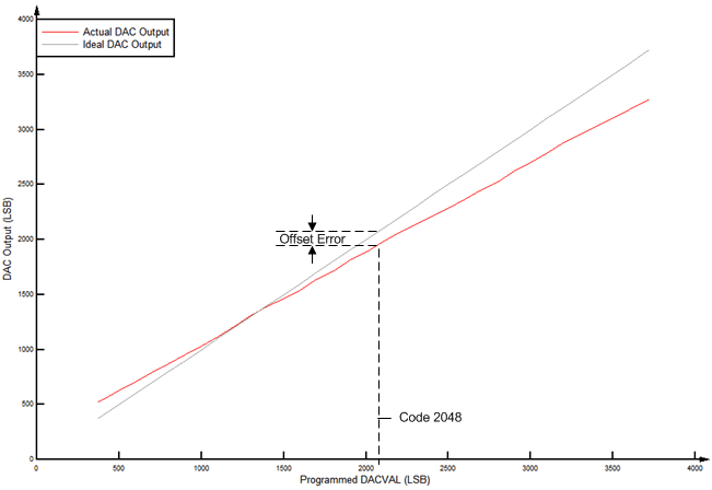
 Figure 4-44 Buffered DAC Offset
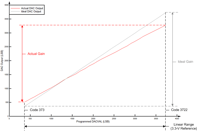
 Figure 4-45 Buffered DAC Gain
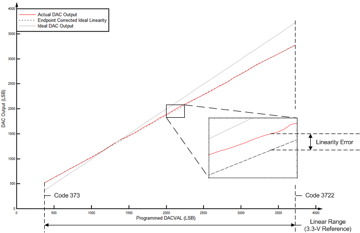
 Figure 4-46 Buffered DAC Linearity