ZHCST39A December 2022 – September 2023 AFE11612-SEP
PRODUCTION DATA
- 1
- 1 特性
- 2 应用
- 3 说明
- 4 Revision History
- 5 Pin Configuration and Functions
-
6 Specifications
- 6.1 Absolute Maximum Ratings
- 6.2 ESD Ratings
- 6.3 Recommended Operating Conditions
- 6.4 Thermal Information
- 6.5 Electrical Characteristics
- 6.6 Timing Characteristics
- 6.7 Timing Diagrams
- 6.8 Typical Characteristics: DAC
- 6.9 Typical Characteristics: ADC
- 6.10 Typical Characteristics: Internal Reference
- 6.11 Typical Characteristics: Temperature Sensor
- 6.12 Typical Characteristics: Digital Inputs
-
7 Detailed Description
- 7.1 Overview
- 7.2 Functional Block Diagram
- 7.3
Feature Description
- 7.3.1
Primary ADC Operation
- 7.3.1.1 Analog Inputs
- 7.3.1.2 ADC Trigger Signals (See AFE configuration register 0 )
- 7.3.1.3 Double-Buffered ADC Data Registers
- 7.3.1.4 SCLK Clock Noise Reduction
- 7.3.1.5 Data Available Pin (DAV)
- 7.3.1.6 Convert Pin (CNVT)
- 7.3.1.7 Analog Input Out-of-Range Detection (See The Analog Input Out-of-Range Alarm Section)
- 7.3.1.8 Full-Scale Range of the Analog Input
- 7.3.2 Secondary ADC and Temperature Sensor Operation
- 7.3.3 Reference Operation
- 7.3.4 DAC Operation
- 7.3.5 Alarm Operation
- 7.3.6 General-Purpose Input and Output Pins (GPIO-0 To GPIO-7)
- 7.3.7 Device Reset Options
- 7.3.1
Primary ADC Operation
- 7.4 Device Functional Modes
- 7.5 Programming
- 7.6
Register Maps
- 7.6.1 Temperature Data Registers (Read-Only)
- 7.6.2 Temperature Configuration (TEMP_CONFIG) Register (address = 0Ah) [reset = 003Ch or 3CFFh]
- 7.6.3 Temperature Conversion Rate (TEMP_CONV_RATE) Register (address = 0Bh) [reset = 0007h or 07FFh]
- 7.6.4 η-Factor Correction Registers: D1_N_ADJUST and D2_N_ADJUST (address = 21h and 22h) [reset = 0000h or 00FFh]
- 7.6.5 ADC-n-Data (ADC_n) Registers (addresses = 23h to 32h) [reset = 0000h]
- 7.6.6 DAC-n-Data (DAC_n) Registers (addresses = 33h to 3Eh) [reset = 0000h)
- 7.6.7 DAC-n-CLR-Setting (DAC_n_CLR) Registers (addresses = 3Fh to 4Ah) [reset = 0000h]
- 7.6.8 GPIO Register (address = 4Bh) [reset = 00FFh]
- 7.6.9 AFE Configuration Register 0 (AFE_CONFIG_0) (address = 4Ch) [reset = 2000h]
- 7.6.10 AFE Configuration Register 1 (AFE_CONFIG_1) (Address = 4Dh) [reset = 0070h]
- 7.6.11 Alarm Control Register (ALR_CTRL) (address = 4Eh) [reset = 0000h]
- 7.6.12 STATUS Register (Address = 4Fh) [reset = 0000h]
- 7.6.13 ADC Channel Register 0 (ADC_CH0) (address = 50h) [reset = 0000h]
- 7.6.14 ADC Channel Register 1 (ADC_CH1) (address = 51h) [reset = 0000h]
- 7.6.15 ADC Gain Register (ADC_GAIN) (address = 52h) [reset = FFFFh]
- 7.6.16 AUTO_DAC_CLR_SOURCE Register (address = 53h) [reset = 0004h]
- 7.6.17 AUTO_DAC_CLR_EN Register (address = 54h) [reset = 0000h]
- 7.6.18 SW_DAC_CLR Register (address = 55h) [reset = 0000h]
- 7.6.19 HW_DAC_CLR_EN_0 Register (address = 56h) [reset = 0000h]
- 7.6.20 HW_DAC_CLR_EN_1 Register (address = 57h) [reset = 0000h]
- 7.6.21 DAC Configuration (DAC_CONFIG) Register (address = 58h) [reset = 0000h]
- 7.6.22 DAC Gain (DAC_GAIN) Register (address = 59h) [reset = 0000h]
- 7.6.23 Analog Input Channel Threshold Registers (addresses = 5Ah To 61h)
- 7.6.24
Temperature Threshold Registers
- 7.6.24.1 LT_HIGH_THRESHOLD Register (address = 62h) [reset = 07FFh, +255.875°C]
- 7.6.24.2 LT_LOW_THRESHOLD Register (address = 63h) [reset = 0800h, –256°C]
- 7.6.24.3 D1_HIGH_THRESHOLD Register (address = 64h) [reset = 07FFh, +255.875°C]
- 7.6.24.4 D1_LOW_THRESHOLD Register (address = 65h) [reset = 0800h, –256°C]
- 7.6.24.5 D2_HIGH_THRESHOLD Register (address = 66h) [reset = 07FFh, +255.875°C]
- 7.6.24.6 D2_LOW_THRESHOLD Register (address = 67h) [reset = 0800h, –256°C]
- 7.6.25 Hysteresis Registers
- 7.6.26 Power-Down Register (PWR_DOWN) (address = 6Bh) [reset = 0000h)
- 7.6.27 Device ID Register (DEVICE_ID) (read only address = 6Ch) [reset = 1220h]
- 7.6.28 Software Reset (SW_RST) Register (read or write address = 7Ch) [reset = N/A)
- 8 Application and Implementation
- 9 Device and Documentation Support
- 10Mechanical, Packaging, and Orderable Information
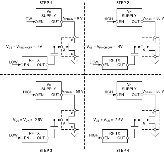
8.2.2.1 Sequencing
Powering the PA on and off in a controlled routine is necessary to prevent the VGS voltage from being too high when the VDRAIN is applied. Such a state causes the PA to operate in saturation mode which can result in thermal damage in the PA or any connected board. Powering on a PA requires the following steps:
- First, apply the VGS signal to the PA. The VGS voltage must transition to the VGS pinch-off voltage or lower. This makes sure that when the VDRAIN voltage is applied, the gate is already low.
- Next, enable the drain voltage supply and allow the VDRAIN to be powered to the nominal value (50 V, for example). As the VGS is at the pinch-off voltage, IDS must be minimal.
- After the VDRAIN is applied, increase the VGS bias voltage to set the desired power output of the PA.
- Finally, enable the RF signal. This allows the PA to transmit a signal.
 Figure 8-2 GaN Power Sequencing
The PA can be safely shut down by reversing the power-on steps.
- Disable the RF signal from the PA.
- Reduce the VGS voltage to the pinch-off value, eliminating the power output of the PA.
- Disable the VDRAIN voltage by sending a disable signal to the drain supply.
- Finally, the VGS voltage can be allowed to collapse to ground as the PA is fully disabled.