ZHCST39A December 2022 – September 2023 AFE11612-SEP
PRODUCTION DATA
- 1
- 1 特性
- 2 应用
- 3 说明
- 4 Revision History
- 5 Pin Configuration and Functions
-
6 Specifications
- 6.1 Absolute Maximum Ratings
- 6.2 ESD Ratings
- 6.3 Recommended Operating Conditions
- 6.4 Thermal Information
- 6.5 Electrical Characteristics
- 6.6 Timing Characteristics
- 6.7 Timing Diagrams
- 6.8 Typical Characteristics: DAC
- 6.9 Typical Characteristics: ADC
- 6.10 Typical Characteristics: Internal Reference
- 6.11 Typical Characteristics: Temperature Sensor
- 6.12 Typical Characteristics: Digital Inputs
-
7 Detailed Description
- 7.1 Overview
- 7.2 Functional Block Diagram
- 7.3
Feature Description
- 7.3.1
Primary ADC Operation
- 7.3.1.1 Analog Inputs
- 7.3.1.2 ADC Trigger Signals (See AFE configuration register 0 )
- 7.3.1.3 Double-Buffered ADC Data Registers
- 7.3.1.4 SCLK Clock Noise Reduction
- 7.3.1.5 Data Available Pin (DAV)
- 7.3.1.6 Convert Pin (CNVT)
- 7.3.1.7 Analog Input Out-of-Range Detection (See The Analog Input Out-of-Range Alarm Section)
- 7.3.1.8 Full-Scale Range of the Analog Input
- 7.3.2 Secondary ADC and Temperature Sensor Operation
- 7.3.3 Reference Operation
- 7.3.4 DAC Operation
- 7.3.5 Alarm Operation
- 7.3.6 General-Purpose Input and Output Pins (GPIO-0 To GPIO-7)
- 7.3.7 Device Reset Options
- 7.3.1
Primary ADC Operation
- 7.4 Device Functional Modes
- 7.5 Programming
- 7.6
Register Maps
- 7.6.1 Temperature Data Registers (Read-Only)
- 7.6.2 Temperature Configuration (TEMP_CONFIG) Register (address = 0Ah) [reset = 003Ch or 3CFFh]
- 7.6.3 Temperature Conversion Rate (TEMP_CONV_RATE) Register (address = 0Bh) [reset = 0007h or 07FFh]
- 7.6.4 η-Factor Correction Registers: D1_N_ADJUST and D2_N_ADJUST (address = 21h and 22h) [reset = 0000h or 00FFh]
- 7.6.5 ADC-n-Data (ADC_n) Registers (addresses = 23h to 32h) [reset = 0000h]
- 7.6.6 DAC-n-Data (DAC_n) Registers (addresses = 33h to 3Eh) [reset = 0000h)
- 7.6.7 DAC-n-CLR-Setting (DAC_n_CLR) Registers (addresses = 3Fh to 4Ah) [reset = 0000h]
- 7.6.8 GPIO Register (address = 4Bh) [reset = 00FFh]
- 7.6.9 AFE Configuration Register 0 (AFE_CONFIG_0) (address = 4Ch) [reset = 2000h]
- 7.6.10 AFE Configuration Register 1 (AFE_CONFIG_1) (Address = 4Dh) [reset = 0070h]
- 7.6.11 Alarm Control Register (ALR_CTRL) (address = 4Eh) [reset = 0000h]
- 7.6.12 STATUS Register (Address = 4Fh) [reset = 0000h]
- 7.6.13 ADC Channel Register 0 (ADC_CH0) (address = 50h) [reset = 0000h]
- 7.6.14 ADC Channel Register 1 (ADC_CH1) (address = 51h) [reset = 0000h]
- 7.6.15 ADC Gain Register (ADC_GAIN) (address = 52h) [reset = FFFFh]
- 7.6.16 AUTO_DAC_CLR_SOURCE Register (address = 53h) [reset = 0004h]
- 7.6.17 AUTO_DAC_CLR_EN Register (address = 54h) [reset = 0000h]
- 7.6.18 SW_DAC_CLR Register (address = 55h) [reset = 0000h]
- 7.6.19 HW_DAC_CLR_EN_0 Register (address = 56h) [reset = 0000h]
- 7.6.20 HW_DAC_CLR_EN_1 Register (address = 57h) [reset = 0000h]
- 7.6.21 DAC Configuration (DAC_CONFIG) Register (address = 58h) [reset = 0000h]
- 7.6.22 DAC Gain (DAC_GAIN) Register (address = 59h) [reset = 0000h]
- 7.6.23 Analog Input Channel Threshold Registers (addresses = 5Ah To 61h)
- 7.6.24
Temperature Threshold Registers
- 7.6.24.1 LT_HIGH_THRESHOLD Register (address = 62h) [reset = 07FFh, +255.875°C]
- 7.6.24.2 LT_LOW_THRESHOLD Register (address = 63h) [reset = 0800h, –256°C]
- 7.6.24.3 D1_HIGH_THRESHOLD Register (address = 64h) [reset = 07FFh, +255.875°C]
- 7.6.24.4 D1_LOW_THRESHOLD Register (address = 65h) [reset = 0800h, –256°C]
- 7.6.24.5 D2_HIGH_THRESHOLD Register (address = 66h) [reset = 07FFh, +255.875°C]
- 7.6.24.6 D2_LOW_THRESHOLD Register (address = 67h) [reset = 0800h, –256°C]
- 7.6.25 Hysteresis Registers
- 7.6.26 Power-Down Register (PWR_DOWN) (address = 6Bh) [reset = 0000h)
- 7.6.27 Device ID Register (DEVICE_ID) (read only address = 6Ch) [reset = 1220h]
- 7.6.28 Software Reset (SW_RST) Register (read or write address = 7Ch) [reset = N/A)
- 8 Application and Implementation
- 9 Device and Documentation Support
- 10Mechanical, Packaging, and Orderable Information
7.3.5.2 ALARM Pin
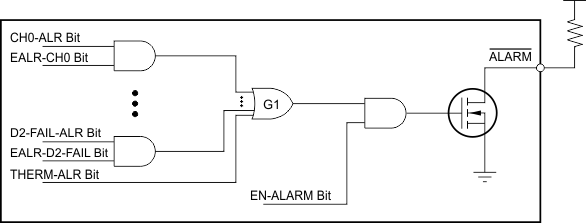
The ALARM pin is a global alarm indicator. ALARM is an open-drain pin, as Figure 7-15 illustrates; an external pullup resistor is required. When the pin is activated, the pin goes low. When the pin is inactive, the pin is in Hi-Z status. The ALARM pin functions as an interrupt to the host so that this pin can query the status register to determine the alarm source. Any alarm event (including analog inputs, temperatures, diode status, and device thermal condition) activates the pin if the alarm is not masked (the corresponding EALR bit in the alarm control register is 1). When the alarm pin is masked (EN-ALARM bit is 0), the occurrence of the event sets the corresponding status bit in status register to 1, but does not activate the ALARM pin.
 Figure 7-15 ALARM Pin
When the ALARM-LATCH-DIS bit in the alarm control register is cleared (0), the alarm is latched. Reading the status register clears the alarm status bit. Whenever an alarm status bit is set, indicating an alarm condition, the bit remains set until the event that caused the alarm is resolved and the status register is read. The alarm bit can only be cleared by reading the status register after the event is resolved, or by a hardware reset, software reset, or power-on reset (POR). All bits are cleared when reading the status register, and all bits are reasserted if the out-of-limit condition still exists after the next conversion cycle, unless otherwise noted. When the ALARM-LATCH-DIS bit in the alarm control register is set (1), the ALARM pin is not latched. The alarm bit clears to 0 when the error condition subsides, regardless of whether the bit is read or not.