ZHCSNC8A February 2021 – March 2021 TPS541620
PRODUCTION DATA
- 1 特性
- 2 应用
- 3 说明
- 4 Revision History
- 5 Pin Configuration and Functions
- 6 Specifications
-
7 Detailed Description
- 7.1 Overview
- 7.2 Functional Block Diagram
- 7.3
Feature Description
- 7.3.1 Fixed-Frequency, Internally Compensated Advanced-Current-Mode Control
- 7.3.2 Enable and UVLO
- 7.3.3 Internal LDO
- 7.3.4 Pre-biased Output Start-up
- 7.3.5 Current Sharing
- 7.3.6 Frequency Selection and Minimum On-Time and Off-Time
- 7.3.7 Ramp Compensation Selection
- 7.3.8 Soft Start
- 7.3.9 Remote Sense Function
- 7.3.10 Adjustable Output Voltage
- 7.3.11 Power Good
- 7.3.12 Overcurrent Protection
- 7.3.13 Overvoltage and Undervoltage Protection
- 7.3.14 Overtemperature Protection
- 7.3.15 Frequency Synchronization
- 7.4 Device Functional Modes
-
8 Application and Implementation
- 8.1 Application Information
- 8.2
Typical Application - Dual Independent Outputs
- 8.2.1 Design Requirements
- 8.2.2
Detailed Design Procedure
- 8.2.2.1 Switching Frequency
- 8.2.2.2 Output Inductor Selection
- 8.2.2.3 Output Capacitor
- 8.2.2.4 Input Capacitor
- 8.2.2.5 Output Voltage Resistors Selection
- 8.2.2.6 Adjustable Undervoltage Lockout
- 8.2.2.7 Bootstrap Capacitor Selection
- 8.2.2.8 BP5 Capacitor Selection
- 8.2.2.9 PGOOD Pullup Resistor
- 8.2.2.10 Current Limit
- 8.2.2.11 Soft-Start Time Selection
- 8.2.2.12 MODE1 and MODE2 Pins
- 8.2.3 Application Curves
- 8.2.4
Typical Application - 2-Phase Operation
- 8.2.4.1 Design Requirements
- 8.2.4.2
Detailed Design Procedure
- 8.2.4.2.1 Switching Frequency
- 8.2.4.2.2 Output Inductor Selection
- 8.2.4.2.3 Output Capacitor
- 8.2.4.2.4 Input Capacitor
- 8.2.4.2.5 Output Voltage Resistors Selection
- 8.2.4.2.6 Adjustable Undervoltage Lockout
- 8.2.4.2.7 Bootstrap Capacitor Selection
- 8.2.4.2.8 BP5 Capacitor Selection
- 8.2.4.2.9 PGOOD Pullup Resistor
- 8.2.4.2.10 Current Limit
- 8.2.4.2.11 Soft-Start Time Selection
- 8.2.4.2.12 MODE1 Pin
- 8.2.4.3 Application Curves
- 9 Power Supply Recommendations
- 10Layout
- 11Device and Documentation Support
- 12Mechanical, Packaging, and Orderable Information
8.2.2.2 Output Inductor Selection
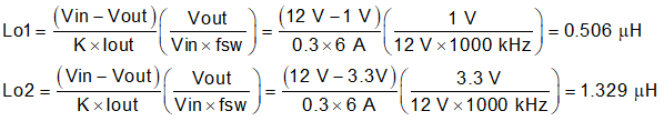
To calculate the effective value of the output inductor, use Equation 24. K is a ratio that represents the amount of inductor ripple current relative to the maximum output current. The inductor ripple current is filtered by the output capacitor. Therefore, choosing high inductor ripple currents impacts the selection of the output capacitor since the output capacitor must have a ripple current rating equal to or greater than the inductor ripple current. Choosing small inductor ripple currents (through a large inductor) can degrade the transient response performance. The inductor ripple, K, is normally 0.1 to 0.4 for the majority of applications, giving a peak-to-peak ripple current range of 0.6 A to 2.4 A. The target Iripple must be 0.3 A or larger.
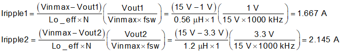
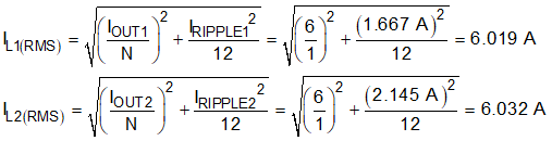
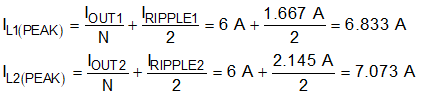
For this design example, K = 0.3 is used and the inductor values Lo1 and Lo2 are calculated to be 0.506 µH and 1.329 µH, respectively. An inductor with an inductance of 0.56 μH is selected for VOUT1 and 1.2 μH for VOUT2. It is important that the RMS (Root Mean Square) current and saturation current ratings of the inductor not be exceeded. The RMS and peak inductor current can be found in Equation 26 and Equation 27, respectively. For VOUT1 in this design, the RMS inductor current is 6.019 A and the peak inductor current is 6.833 A. The chosen inductor is a Coilcraft XAL6030-561. For VOUT2 in this design, the RMS inductor current is 6.032 A and the peak inductor current is 7.073 A. The chosen inductor for VOUT2 is a Coilcraft XAL6030-122. XAL6030-561 has a saturation current rating of 29 A, an RMS current rating of 17 A, and a typical DC series resistance of 3.01 mΩ. The XAL6030-122 has a saturation current rating of 22 A, an RMS current rating of 13 A, and a typical DC series resistance of 6.8 mΩ.
The peak current through the inductor is the inductor ripple current plus the DC output current. During power up, faults, or transient load conditions, the inductor current can increase above the calculated peak inductor current level calculated in Equation 27. In transient conditions, the inductor current can increase up to the switch current limit of the device. For this reason, the most conservative approach is to specify the current ratings of the inductor based on the switch current limit rather than the steady-state peak inductor current.