ZHCSNC8A February 2021 – March 2021 TPS541620
PRODUCTION DATA
- 1 特性
- 2 应用
- 3 说明
- 4 Revision History
- 5 Pin Configuration and Functions
- 6 Specifications
-
7 Detailed Description
- 7.1 Overview
- 7.2 Functional Block Diagram
- 7.3
Feature Description
- 7.3.1 Fixed-Frequency, Internally Compensated Advanced-Current-Mode Control
- 7.3.2 Enable and UVLO
- 7.3.3 Internal LDO
- 7.3.4 Pre-biased Output Start-up
- 7.3.5 Current Sharing
- 7.3.6 Frequency Selection and Minimum On-Time and Off-Time
- 7.3.7 Ramp Compensation Selection
- 7.3.8 Soft Start
- 7.3.9 Remote Sense Function
- 7.3.10 Adjustable Output Voltage
- 7.3.11 Power Good
- 7.3.12 Overcurrent Protection
- 7.3.13 Overvoltage and Undervoltage Protection
- 7.3.14 Overtemperature Protection
- 7.3.15 Frequency Synchronization
- 7.4 Device Functional Modes
-
8 Application and Implementation
- 8.1 Application Information
- 8.2
Typical Application - Dual Independent Outputs
- 8.2.1 Design Requirements
- 8.2.2
Detailed Design Procedure
- 8.2.2.1 Switching Frequency
- 8.2.2.2 Output Inductor Selection
- 8.2.2.3 Output Capacitor
- 8.2.2.4 Input Capacitor
- 8.2.2.5 Output Voltage Resistors Selection
- 8.2.2.6 Adjustable Undervoltage Lockout
- 8.2.2.7 Bootstrap Capacitor Selection
- 8.2.2.8 BP5 Capacitor Selection
- 8.2.2.9 PGOOD Pullup Resistor
- 8.2.2.10 Current Limit
- 8.2.2.11 Soft-Start Time Selection
- 8.2.2.12 MODE1 and MODE2 Pins
- 8.2.3 Application Curves
- 8.2.4
Typical Application - 2-Phase Operation
- 8.2.4.1 Design Requirements
- 8.2.4.2
Detailed Design Procedure
- 8.2.4.2.1 Switching Frequency
- 8.2.4.2.2 Output Inductor Selection
- 8.2.4.2.3 Output Capacitor
- 8.2.4.2.4 Input Capacitor
- 8.2.4.2.5 Output Voltage Resistors Selection
- 8.2.4.2.6 Adjustable Undervoltage Lockout
- 8.2.4.2.7 Bootstrap Capacitor Selection
- 8.2.4.2.8 BP5 Capacitor Selection
- 8.2.4.2.9 PGOOD Pullup Resistor
- 8.2.4.2.10 Current Limit
- 8.2.4.2.11 Soft-Start Time Selection
- 8.2.4.2.12 MODE1 Pin
- 8.2.4.3 Application Curves
- 9 Power Supply Recommendations
- 10Layout
- 11Device and Documentation Support
- 12Mechanical, Packaging, and Orderable Information
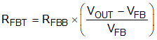
7.3.10 Adjustable Output Voltage
The voltage regulation loop in the TPS541620 regulates the FB pin voltage to be equal to the internal reference voltage. The output voltage of the TPS541620 is set by a resistor divider to program the ratio from VOUT to VFB. The resistor divider is connected from the output to ground with the mid-point connecting to the FB pin (VFB = 0.5 V).
The internal voltage reference and feedback loop produce precise voltage regulation over temperature. TI recommends using divider resistors with 1% tolerance or better, and with a temperature coefficient of 100 ppm or lower for increased DC accuracy over temperature. Typically, RFBT (top feedback resistor) equal to 10 kΩ to 100 kΩ is recommended. Larger RFBT and RFBB (bottom feedback resistor) values reduce the quiescent current going through the divider, which helps maintain high efficiency at very light load. However, larger divider values also make the feedback path more susceptible to noise. RFBB can be calculated by Equation 2.