ZHCSNC8A February 2021 – March 2021 TPS541620
PRODUCTION DATA
- 1 特性
- 2 应用
- 3 说明
- 4 Revision History
- 5 Pin Configuration and Functions
- 6 Specifications
-
7 Detailed Description
- 7.1 Overview
- 7.2 Functional Block Diagram
- 7.3
Feature Description
- 7.3.1 Fixed-Frequency, Internally Compensated Advanced-Current-Mode Control
- 7.3.2 Enable and UVLO
- 7.3.3 Internal LDO
- 7.3.4 Pre-biased Output Start-up
- 7.3.5 Current Sharing
- 7.3.6 Frequency Selection and Minimum On-Time and Off-Time
- 7.3.7 Ramp Compensation Selection
- 7.3.8 Soft Start
- 7.3.9 Remote Sense Function
- 7.3.10 Adjustable Output Voltage
- 7.3.11 Power Good
- 7.3.12 Overcurrent Protection
- 7.3.13 Overvoltage and Undervoltage Protection
- 7.3.14 Overtemperature Protection
- 7.3.15 Frequency Synchronization
- 7.4 Device Functional Modes
-
8 Application and Implementation
- 8.1 Application Information
- 8.2
Typical Application - Dual Independent Outputs
- 8.2.1 Design Requirements
- 8.2.2
Detailed Design Procedure
- 8.2.2.1 Switching Frequency
- 8.2.2.2 Output Inductor Selection
- 8.2.2.3 Output Capacitor
- 8.2.2.4 Input Capacitor
- 8.2.2.5 Output Voltage Resistors Selection
- 8.2.2.6 Adjustable Undervoltage Lockout
- 8.2.2.7 Bootstrap Capacitor Selection
- 8.2.2.8 BP5 Capacitor Selection
- 8.2.2.9 PGOOD Pullup Resistor
- 8.2.2.10 Current Limit
- 8.2.2.11 Soft-Start Time Selection
- 8.2.2.12 MODE1 and MODE2 Pins
- 8.2.3 Application Curves
- 8.2.4
Typical Application - 2-Phase Operation
- 8.2.4.1 Design Requirements
- 8.2.4.2
Detailed Design Procedure
- 8.2.4.2.1 Switching Frequency
- 8.2.4.2.2 Output Inductor Selection
- 8.2.4.2.3 Output Capacitor
- 8.2.4.2.4 Input Capacitor
- 8.2.4.2.5 Output Voltage Resistors Selection
- 8.2.4.2.6 Adjustable Undervoltage Lockout
- 8.2.4.2.7 Bootstrap Capacitor Selection
- 8.2.4.2.8 BP5 Capacitor Selection
- 8.2.4.2.9 PGOOD Pullup Resistor
- 8.2.4.2.10 Current Limit
- 8.2.4.2.11 Soft-Start Time Selection
- 8.2.4.2.12 MODE1 Pin
- 8.2.4.3 Application Curves
- 9 Power Supply Recommendations
- 10Layout
- 11Device and Documentation Support
- 12Mechanical, Packaging, and Orderable Information
7.3.2 Enable and UVLO
The precision enable feature of the TPS541620 allows the voltage on the EN1/EN2 pin (VEN) to control the ON/OFF functionality of the device. The EN pin has a 1.4-μA typical internal pullup current source. Floating the EN pin allows the device to start up when a valid input voltage is applied. The TPS541620 switching action and output regulation are enabled when VEN is greater than 1.2 V (typical). While the device is switching, if the EN voltage falls below 1.1 V (typical), the device stops switching.
It is recommended to enable the device at a voltage greater than the minimum input voltage. Control the turn-on and turn-off using a resistor divider on the EN1 (EN2) pin, between VIN and AGND (see Figure 7-1). Set the divider to a voltage greater than the minimum input voltage as shown in Figure 7-2. Select a top enable resistor of 100 kΩ and use Equation 1 for RENB selection. It is recommended to use divider resistors with 1% tolerance or better and with a temperature coefficient of 100 ppm or lower.
The minimum input voltage of the TPS541620 is 4.5 V, however, the minimum input voltage increases at higher output voltages. Figure 7-2 plots the minimum required input voltage for each of the allowable switching frequencies across the output voltage range. It is recommended to control the turn-on and turn-off of the device at an input voltage greater than the minimum shown in Figure 7-2 using a resistor divider on the EN1 (EN2) pin, between VIN and AGND (see Figure 7-1).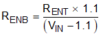
 Figure 7-1 Enable ON/OFF Control