ZHCSI27C April 2018 – October 2021 LM5036
PRODUCTION DATA
- 1 特性
- 2 应用
- 3 说明
- 4 Revision History
- 5 Pin Configuration and Functions
- 6 Specifications
-
7 Detailed Description
- 7.1 Overview
- 7.2 Functional Block Diagram
- 7.3
Feature Description
- 7.3.1 High-Voltage Start-Up Regulator
- 7.3.2 Undervoltage Lockout (UVLO)
- 7.3.3 Reference Regulator
- 7.3.4 Oscillator, Synchronized Input
- 7.3.5 Voltage-Mode Control
- 7.3.6 Primary-Side Gate Driver Outputs (LSG and HSG)
- 7.3.7 Half-Bridge PWM Scheme
- 7.3.8 Maximum Duty Cycle Operation
- 7.3.9 Pre-Biased Start-Up Process
- 7.3.10 Zero Duty Cycle Operation
- 7.3.11 Enhanced Cycle-by-Cycle Current Limiting with Pulse Matching
- 7.3.12 Reverse Current Protection
- 7.3.13 CBC Threshold Accuracy
- 7.3.14 Hiccup Mode Protection
- 7.3.15 Hiccup Mode Blanking
- 7.3.16 Over-Temperature Protection (OTP)
- 7.3.17 Over-Voltage / Latch (ON_OFF Pin)
- 7.3.18 Auxiliary Constant On-Time Control
- 7.3.19 Auxiliary On-Time Generator
- 7.3.20 Auxiliary Supply Current Limiting
- 7.3.21 Auxiliary Primary Output Capacitor Ripple
- 7.3.22 Auxiliary Ripple Configuration and Control
- 7.3.23 Asynchronous Mode Operation of Auxiliary Supply
- 7.4 Device Functional Modes
-
8 Application and Implementation
- 8.1 Application Information
- 8.2
Typical Application
- 8.2.1 Design Requirements
- 8.2.2
Detailed Design Procedure
- 8.2.2.1 Custom Design With WEBENCH® Tools
- 8.2.2.2 Input Transient Protection
- 8.2.2.3 Level-Shift Detection Circuit
- 8.2.2.4 Applications with VIN > 100-V
- 8.2.2.5 Applications without Pre-Biased Start-Up Requirement
- 8.2.2.6 UVLO Voltage Divider Selection
- 8.2.2.7 Over Voltage, Latch (ON_OFF Pin) Voltage Divider Selection
- 8.2.2.8 SS Capacitor
- 8.2.2.9 SSSR Capacitor
- 8.2.2.10 Half-Bridge Power Stage Design
- 8.2.2.11 Current Limit
- 8.2.2.12 Auxiliary Transformer
- 8.2.2.13 Auxiliary Feedback Resistors
- 8.2.2.14 RON Resistor
- 8.2.2.15 VIN Pin Capacitor
- 8.2.2.16 Auxiliary Primary Output Capacitor
- 8.2.2.17 Auxiliary Secondary Output Capacitor
- 8.2.2.18 Auxiliary Feedback Ripple Circuit
- 8.2.2.19 Auxiliary Secondary Diode
- 8.2.2.20 VCC Diode
- 8.2.2.21 Opto-Coupler Interface
- 8.2.2.22 Full-Bridge Converter Applications
- 8.2.3 Application Curves
- 9 Power Supply Recommendations
- 10Layout
- 11Device and Documentation Support
- 12Mechanical, Packaging, and Orderable Information
8.2.2.12 Auxiliary Transformer
A coupled inductor or a flyback-type transformer is required for this fly-buck topology auxiliary supply. Energy is transferred from primary to secondary when the low-side SR MOSFET is conducting.
The transformer turns ratio is selected based on the ratio of the primary output voltage to the secondary output voltage. In this design example, the two outputs are set to be equal and a 1:1 turns ratio transformer is selected, i.e., N2/N1 = 1. The primary output voltage is normally selected based on the input voltage range such that the duty cycle of the converter does not exceed 50% at the minimum input voltage. This condition is satisfied if VAUX1 < VIN(min) / 2.
Use Equation 86 to calculate the maximum inductor current ripple amplitude ΔIL(AUX) that can be tolerated without exceeding the peak current limit threshold IAUX(LIM) (200-mA typical) of the high-side switch,
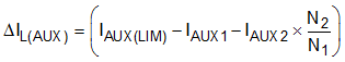
where
- IAUX1 is the primary output current, and IAUX2 is the secondary output current of the auxiliary supply, respectively.
In this design example, the maximum total output current IAUX(max) of the auxiliary supply referred to the primary side is 100-mA, as given by Equation 87.

Therefore, ΔIL(AUX) = 0.1-A. Use Equation 88 to calculate the minimum inductor value for the auxiliary supply.
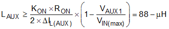
Select a higher value of 150-µH to ensure the high-side switch current doesn’t exceed the minimum peak current limit threshold.