ZHCSI27C April 2018 – October 2021 LM5036
PRODUCTION DATA
- 1 特性
- 2 应用
- 3 说明
- 4 Revision History
- 5 Pin Configuration and Functions
- 6 Specifications
-
7 Detailed Description
- 7.1 Overview
- 7.2 Functional Block Diagram
- 7.3
Feature Description
- 7.3.1 High-Voltage Start-Up Regulator
- 7.3.2 Undervoltage Lockout (UVLO)
- 7.3.3 Reference Regulator
- 7.3.4 Oscillator, Synchronized Input
- 7.3.5 Voltage-Mode Control
- 7.3.6 Primary-Side Gate Driver Outputs (LSG and HSG)
- 7.3.7 Half-Bridge PWM Scheme
- 7.3.8 Maximum Duty Cycle Operation
- 7.3.9 Pre-Biased Start-Up Process
- 7.3.10 Zero Duty Cycle Operation
- 7.3.11 Enhanced Cycle-by-Cycle Current Limiting with Pulse Matching
- 7.3.12 Reverse Current Protection
- 7.3.13 CBC Threshold Accuracy
- 7.3.14 Hiccup Mode Protection
- 7.3.15 Hiccup Mode Blanking
- 7.3.16 Over-Temperature Protection (OTP)
- 7.3.17 Over-Voltage / Latch (ON_OFF Pin)
- 7.3.18 Auxiliary Constant On-Time Control
- 7.3.19 Auxiliary On-Time Generator
- 7.3.20 Auxiliary Supply Current Limiting
- 7.3.21 Auxiliary Primary Output Capacitor Ripple
- 7.3.22 Auxiliary Ripple Configuration and Control
- 7.3.23 Asynchronous Mode Operation of Auxiliary Supply
- 7.4 Device Functional Modes
-
8 Application and Implementation
- 8.1 Application Information
- 8.2
Typical Application
- 8.2.1 Design Requirements
- 8.2.2
Detailed Design Procedure
- 8.2.2.1 Custom Design With WEBENCH® Tools
- 8.2.2.2 Input Transient Protection
- 8.2.2.3 Level-Shift Detection Circuit
- 8.2.2.4 Applications with VIN > 100-V
- 8.2.2.5 Applications without Pre-Biased Start-Up Requirement
- 8.2.2.6 UVLO Voltage Divider Selection
- 8.2.2.7 Over Voltage, Latch (ON_OFF Pin) Voltage Divider Selection
- 8.2.2.8 SS Capacitor
- 8.2.2.9 SSSR Capacitor
- 8.2.2.10 Half-Bridge Power Stage Design
- 8.2.2.11 Current Limit
- 8.2.2.12 Auxiliary Transformer
- 8.2.2.13 Auxiliary Feedback Resistors
- 8.2.2.14 RON Resistor
- 8.2.2.15 VIN Pin Capacitor
- 8.2.2.16 Auxiliary Primary Output Capacitor
- 8.2.2.17 Auxiliary Secondary Output Capacitor
- 8.2.2.18 Auxiliary Feedback Ripple Circuit
- 8.2.2.19 Auxiliary Secondary Diode
- 8.2.2.20 VCC Diode
- 8.2.2.21 Opto-Coupler Interface
- 8.2.2.22 Full-Bridge Converter Applications
- 8.2.3 Application Curves
- 9 Power Supply Recommendations
- 10Layout
- 11Device and Documentation Support
- 12Mechanical, Packaging, and Orderable Information
7.3.13 CBC Threshold Accuracy
The CBC current limit amplifier deployed within LM5036 is a precise component. In common with all such devices the input bias currents and input offset voltage will lead to small variations in the current trip threshold between parts and across temperature.
 Figure 7-16 Diagram of Current Limiting Function with Error Terms Shown in Red
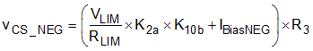
At its trip threshold the two inputs of the CBC comparator must be equal. At this condition the voltage on the CS_NEG pin is given by Equation 17.
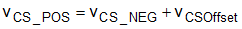
The voltage drop across the ideal amplifier input must be zero. The voltage of the CS_POS pin, at the trip threshold can be expressed as follows:

Combining Equation 17, Equation 18 and Equation 19 and re-arranging gives an expression for the voltage across the current sense resistor at the trip threshold Equation 20.
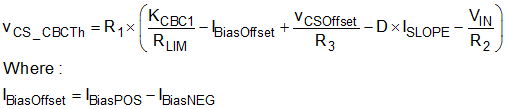
Hence, for a given set of external component values, the variation in current trip threshold across parts and temperature can be found using data supplied in the Electrical Tables.
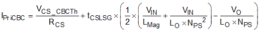
A short delay will exist (tCSLSG), after the CBC comparator inputs reach their trip threshold, before the LSG falling edge. During this delay the primary current will continue to ramp, giving rise to a further error in the apparent trip threshold. The peak primary current flowing when the low side MOSFET switches OFF (IPriCBC), is expressed by Equation 21.
The output current at which the primary peak current threshold is reached is expressed by Equation 22.
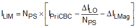
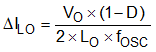
ΔILO is the amplitude of ripple current in the output inductor and is expressed in Equation 23.
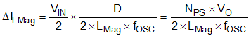
ΔILMag is the amplitude of ripple current in the magnetising inductor and is expressed in Equation 24.
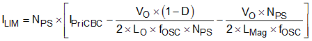
Combining Equation 22, Equation 23 and Equation 24 gives an expression for output current limit as a function of primary current limit threshold Equation 25.
The Excel Calculator Tool can be used to evaluate the tolerance of output current limit.