ZHCSI27C April 2018 – October 2021 LM5036
PRODUCTION DATA
- 1 特性
- 2 应用
- 3 说明
- 4 Revision History
- 5 Pin Configuration and Functions
- 6 Specifications
-
7 Detailed Description
- 7.1 Overview
- 7.2 Functional Block Diagram
- 7.3
Feature Description
- 7.3.1 High-Voltage Start-Up Regulator
- 7.3.2 Undervoltage Lockout (UVLO)
- 7.3.3 Reference Regulator
- 7.3.4 Oscillator, Synchronized Input
- 7.3.5 Voltage-Mode Control
- 7.3.6 Primary-Side Gate Driver Outputs (LSG and HSG)
- 7.3.7 Half-Bridge PWM Scheme
- 7.3.8 Maximum Duty Cycle Operation
- 7.3.9 Pre-Biased Start-Up Process
- 7.3.10 Zero Duty Cycle Operation
- 7.3.11 Enhanced Cycle-by-Cycle Current Limiting with Pulse Matching
- 7.3.12 Reverse Current Protection
- 7.3.13 CBC Threshold Accuracy
- 7.3.14 Hiccup Mode Protection
- 7.3.15 Hiccup Mode Blanking
- 7.3.16 Over-Temperature Protection (OTP)
- 7.3.17 Over-Voltage / Latch (ON_OFF Pin)
- 7.3.18 Auxiliary Constant On-Time Control
- 7.3.19 Auxiliary On-Time Generator
- 7.3.20 Auxiliary Supply Current Limiting
- 7.3.21 Auxiliary Primary Output Capacitor Ripple
- 7.3.22 Auxiliary Ripple Configuration and Control
- 7.3.23 Asynchronous Mode Operation of Auxiliary Supply
- 7.4 Device Functional Modes
-
8 Application and Implementation
- 8.1 Application Information
- 8.2
Typical Application
- 8.2.1 Design Requirements
- 8.2.2
Detailed Design Procedure
- 8.2.2.1 Custom Design With WEBENCH® Tools
- 8.2.2.2 Input Transient Protection
- 8.2.2.3 Level-Shift Detection Circuit
- 8.2.2.4 Applications with VIN > 100-V
- 8.2.2.5 Applications without Pre-Biased Start-Up Requirement
- 8.2.2.6 UVLO Voltage Divider Selection
- 8.2.2.7 Over Voltage, Latch (ON_OFF Pin) Voltage Divider Selection
- 8.2.2.8 SS Capacitor
- 8.2.2.9 SSSR Capacitor
- 8.2.2.10 Half-Bridge Power Stage Design
- 8.2.2.11 Current Limit
- 8.2.2.12 Auxiliary Transformer
- 8.2.2.13 Auxiliary Feedback Resistors
- 8.2.2.14 RON Resistor
- 8.2.2.15 VIN Pin Capacitor
- 8.2.2.16 Auxiliary Primary Output Capacitor
- 8.2.2.17 Auxiliary Secondary Output Capacitor
- 8.2.2.18 Auxiliary Feedback Ripple Circuit
- 8.2.2.19 Auxiliary Secondary Diode
- 8.2.2.20 VCC Diode
- 8.2.2.21 Opto-Coupler Interface
- 8.2.2.22 Full-Bridge Converter Applications
- 8.2.3 Application Curves
- 9 Power Supply Recommendations
- 10Layout
- 11Device and Documentation Support
- 12Mechanical, Packaging, and Orderable Information
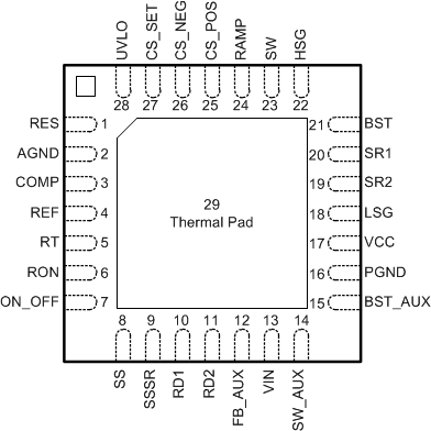
5 Pin Configuration and Functions
 Figure 5-1 RJB Package, 28-Pin WQFN (Top
View)
Figure 5-1 RJB Package, 28-Pin WQFN (Top
View)Table 5-1 Pin Functions
| PIN | TYPE(1) | DESCRIPTION | |
|---|---|---|---|
| NAME | NO. | ||
| AGND | 2 | G | Analog ground |
| BST | 21 | I | Half-bridge high-side gate drive bootstrap |
| BST_AUX | 15 | I | Auxiliary supply high-side gate drive bootstrap |
| COMP | 3 | I | Control current input to half-bridge PWM comparator |
| CS_NEG | 26 | I | Current sense amplifier negative input terminal |
| CS_POS | 25 | I | Current sense amplifier positive input terminal |
| CS_SET | 27 | I | Current limit setting |
| FB_AUX | 12 | I | Auxiliary supply output voltage feedback |
| HSG | 22 | O | Half-bridge high-side MOSFET output driver |
| LSG | 18 | O | Half-bridge low-side MOSFET output driver |
| ON_OFF | 7 | I | Configurable for over voltage protection (OVP) or latch mode |
| PGND | 16 | G | Power ground |
| RAMP | 24 | I | RAMP signal input to half-bridge PWM comparator |
| RD1 | 10 | I | Synchronous rectifier trailing-edge delay |
| RD2 | 11 | I | Synchronous rectifier leading-edge delay |
| REF | 4 | O | 5-V reference regulator output |
| RES | 1 | I | Hiccup mode restart timer |
| RON | 6 | I | Auxiliary supply on-time control |
| RT/SYNC | 5 | I | Oscillator frequency control or external clock synchronization |
| SR1 | 20 | O | Synchronous rectifier PWM control output |
| SR2 | 19 | O | Synchronous rectifier PWM control output |
| SS | 8 | I | Soft-start input |
| SSSR | 9 | I | Synchronous rectifier soft-start input |
| SW | 23 | I | Half-bridge switch node |
| SW_AUX | 14 | I | Auxiliary supply switch node |
| UVLO | 28 | I | Input undervoltage lockout |
| VCC | 17 | I | Bias supply |
| VIN | 13 | I | Input voltage |
| Pad | 29 | G | Exposed thermal pad |
(1) I = Input, O = Output, I/O =
Input or Output, G = Ground, P = Power.