ZHCSI27C April 2018 – October 2021 LM5036
PRODUCTION DATA
- 1 特性
- 2 应用
- 3 说明
- 4 Revision History
- 5 Pin Configuration and Functions
- 6 Specifications
-
7 Detailed Description
- 7.1 Overview
- 7.2 Functional Block Diagram
- 7.3
Feature Description
- 7.3.1 High-Voltage Start-Up Regulator
- 7.3.2 Undervoltage Lockout (UVLO)
- 7.3.3 Reference Regulator
- 7.3.4 Oscillator, Synchronized Input
- 7.3.5 Voltage-Mode Control
- 7.3.6 Primary-Side Gate Driver Outputs (LSG and HSG)
- 7.3.7 Half-Bridge PWM Scheme
- 7.3.8 Maximum Duty Cycle Operation
- 7.3.9 Pre-Biased Start-Up Process
- 7.3.10 Zero Duty Cycle Operation
- 7.3.11 Enhanced Cycle-by-Cycle Current Limiting with Pulse Matching
- 7.3.12 Reverse Current Protection
- 7.3.13 CBC Threshold Accuracy
- 7.3.14 Hiccup Mode Protection
- 7.3.15 Hiccup Mode Blanking
- 7.3.16 Over-Temperature Protection (OTP)
- 7.3.17 Over-Voltage / Latch (ON_OFF Pin)
- 7.3.18 Auxiliary Constant On-Time Control
- 7.3.19 Auxiliary On-Time Generator
- 7.3.20 Auxiliary Supply Current Limiting
- 7.3.21 Auxiliary Primary Output Capacitor Ripple
- 7.3.22 Auxiliary Ripple Configuration and Control
- 7.3.23 Asynchronous Mode Operation of Auxiliary Supply
- 7.4 Device Functional Modes
-
8 Application and Implementation
- 8.1 Application Information
- 8.2
Typical Application
- 8.2.1 Design Requirements
- 8.2.2
Detailed Design Procedure
- 8.2.2.1 Custom Design With WEBENCH® Tools
- 8.2.2.2 Input Transient Protection
- 8.2.2.3 Level-Shift Detection Circuit
- 8.2.2.4 Applications with VIN > 100-V
- 8.2.2.5 Applications without Pre-Biased Start-Up Requirement
- 8.2.2.6 UVLO Voltage Divider Selection
- 8.2.2.7 Over Voltage, Latch (ON_OFF Pin) Voltage Divider Selection
- 8.2.2.8 SS Capacitor
- 8.2.2.9 SSSR Capacitor
- 8.2.2.10 Half-Bridge Power Stage Design
- 8.2.2.11 Current Limit
- 8.2.2.12 Auxiliary Transformer
- 8.2.2.13 Auxiliary Feedback Resistors
- 8.2.2.14 RON Resistor
- 8.2.2.15 VIN Pin Capacitor
- 8.2.2.16 Auxiliary Primary Output Capacitor
- 8.2.2.17 Auxiliary Secondary Output Capacitor
- 8.2.2.18 Auxiliary Feedback Ripple Circuit
- 8.2.2.19 Auxiliary Secondary Diode
- 8.2.2.20 VCC Diode
- 8.2.2.21 Opto-Coupler Interface
- 8.2.2.22 Full-Bridge Converter Applications
- 8.2.3 Application Curves
- 9 Power Supply Recommendations
- 10Layout
- 11Device and Documentation Support
- 12Mechanical, Packaging, and Orderable Information
7.3.17 Over-Voltage / Latch (ON_OFF Pin)
The ON_OFF pin can be configured as a latch pin or OVP pin. In the latch configuration, the half-bridge converter remains off even after the faults are cleared. A new soft-start sequence will not be initiated until the latch is reset. One latch configuration is illustrated in Figure 7-20 where a large latch resistor RL (for example, 50 kΩ) and a diode are tied to the ON_OFF pin.
 Figure 7-20 ON/OFF Pin Latch Function
When any of the faults is detected including OVP, hiccup mode OCP and 150 °C OTP, the ON_OFF pin current source, IOVL (50-µA typical), is activated, that raises the ON_OFF pin voltage quickly. As a result, the latch diode is reverse biased. The current source IOVL remains active even if the fault is cleared because the ON_OFF pin voltage is latched above VON_OFF (1.25-V typical). To reset the latch operation, simply pulling down the UVLO pin voltage below VON_OFF disables the current source and thus the ON_OFF pin voltage falls quickly. A new soft-start sequence will be initiated as soon as the latch is reset and the faults are cleared.
Use Equation 28 to design the external voltage divider in latch mode.
where
- VF is the forward voltage drop of the latch diode
- VIN_L is the desired input voltage latch threshold, and RL is the latch resistor.
Note that the current source IOVL does not provide any hysteresis when ON_OFF pin is configured in latch mode.
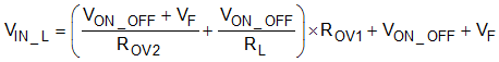
The ON_OFF pin can also be configured as an OVP pin as shown in Figure 7-21. In this configuration, the external voltage divider should be designed such that the ON_OFF pin voltage is greater than VON_OFF when an over-voltage condition occurs.
 Figure 7-21 ON/OFF Pin Configured as OVP Pin
The OVP hysteresis is accomplished with the IOVL current source. When the ON_OFF pin voltage exceeds VON_OFF, the IOVL current source is activated which quickly raises the voltage at the pin. The half-bridge converter is turned off and the SS and SSSR capacitors are fully discharged. When the ON_OFF pin voltage falls below VON_OFF, the current source is deactivated causing the voltage at the pin to quickly fall followed by a new soft-start sequence. In addition to the OVP fault, hiccup mode and internal 150-°C thermal shutdown faults will also cause the half-bridge converter to turn off. Once the faults are cleared, a new soft-start sequence automatically begins. Because the hiccup mode or 150-°C thermal shutdown fault also activates the current source, it is important to make sure that the ON_OFF pin voltage doesn't rise above VON_OFF when the input voltage is high, which otherwise would lead to latch operation. Avoid this scenario by selecting a proper voltage divider.
Use Equation 29 and Equation 30 to select the voltage divider for the OVP configuration.
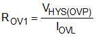
where
- VHYS(OVP) is the OVP hysteresis
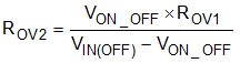
where
- VIN(OFF) is the OVP rising threshold