ZHCSI27C April 2018 – October 2021 LM5036
PRODUCTION DATA
- 1 特性
- 2 应用
- 3 说明
- 4 Revision History
- 5 Pin Configuration and Functions
- 6 Specifications
-
7 Detailed Description
- 7.1 Overview
- 7.2 Functional Block Diagram
- 7.3
Feature Description
- 7.3.1 High-Voltage Start-Up Regulator
- 7.3.2 Undervoltage Lockout (UVLO)
- 7.3.3 Reference Regulator
- 7.3.4 Oscillator, Synchronized Input
- 7.3.5 Voltage-Mode Control
- 7.3.6 Primary-Side Gate Driver Outputs (LSG and HSG)
- 7.3.7 Half-Bridge PWM Scheme
- 7.3.8 Maximum Duty Cycle Operation
- 7.3.9 Pre-Biased Start-Up Process
- 7.3.10 Zero Duty Cycle Operation
- 7.3.11 Enhanced Cycle-by-Cycle Current Limiting with Pulse Matching
- 7.3.12 Reverse Current Protection
- 7.3.13 CBC Threshold Accuracy
- 7.3.14 Hiccup Mode Protection
- 7.3.15 Hiccup Mode Blanking
- 7.3.16 Over-Temperature Protection (OTP)
- 7.3.17 Over-Voltage / Latch (ON_OFF Pin)
- 7.3.18 Auxiliary Constant On-Time Control
- 7.3.19 Auxiliary On-Time Generator
- 7.3.20 Auxiliary Supply Current Limiting
- 7.3.21 Auxiliary Primary Output Capacitor Ripple
- 7.3.22 Auxiliary Ripple Configuration and Control
- 7.3.23 Asynchronous Mode Operation of Auxiliary Supply
- 7.4 Device Functional Modes
-
8 Application and Implementation
- 8.1 Application Information
- 8.2
Typical Application
- 8.2.1 Design Requirements
- 8.2.2
Detailed Design Procedure
- 8.2.2.1 Custom Design With WEBENCH® Tools
- 8.2.2.2 Input Transient Protection
- 8.2.2.3 Level-Shift Detection Circuit
- 8.2.2.4 Applications with VIN > 100-V
- 8.2.2.5 Applications without Pre-Biased Start-Up Requirement
- 8.2.2.6 UVLO Voltage Divider Selection
- 8.2.2.7 Over Voltage, Latch (ON_OFF Pin) Voltage Divider Selection
- 8.2.2.8 SS Capacitor
- 8.2.2.9 SSSR Capacitor
- 8.2.2.10 Half-Bridge Power Stage Design
- 8.2.2.11 Current Limit
- 8.2.2.12 Auxiliary Transformer
- 8.2.2.13 Auxiliary Feedback Resistors
- 8.2.2.14 RON Resistor
- 8.2.2.15 VIN Pin Capacitor
- 8.2.2.16 Auxiliary Primary Output Capacitor
- 8.2.2.17 Auxiliary Secondary Output Capacitor
- 8.2.2.18 Auxiliary Feedback Ripple Circuit
- 8.2.2.19 Auxiliary Secondary Diode
- 8.2.2.20 VCC Diode
- 8.2.2.21 Opto-Coupler Interface
- 8.2.2.22 Full-Bridge Converter Applications
- 8.2.3 Application Curves
- 9 Power Supply Recommendations
- 10Layout
- 11Device and Documentation Support
- 12Mechanical, Packaging, and Orderable Information
7.3.9.1 Primary FETs Soft-Start Process
Figure 7-8 shows a simplified block diagram of the soft-start function.
 Figure 7-8 Soft-Start Function
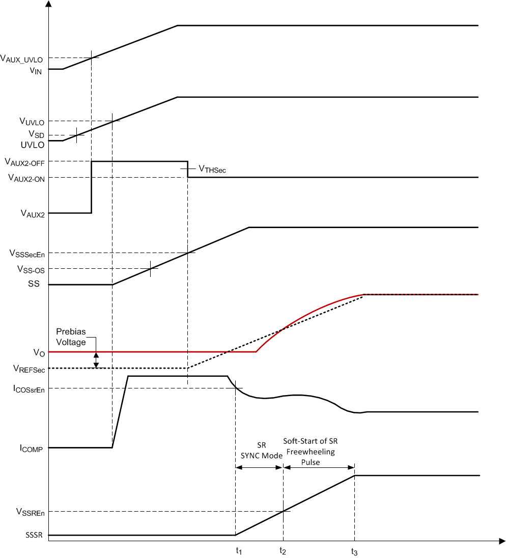
The auxiliary supply has two reference output voltage levels of VAUX-OFF (1.4 -V typical, off state) and VAUX-ON (1-V typical, on state) which facilitates easy voltage level shift detection on the secondary side. The auxiliary supply starts to operate as soon as VIN > VAUX_UVLO (15-V typical) and VCC and REF are above the respective UV thresholds. When the soft-start capacitor is below VSSSecEn (2.06-V typical), the auxiliary supply will produce the off-state voltage on the primary (VAUX1-OFF) and secondary side (VAUX2-OFF), as shown in Figure 7-9.
The off-state auxiliary output voltage level present on the secondary side VAUX2-OFF is above the threshold VTHSec, which activates a reset circuit that discharges the output voltage reference VREFSec. This ensures that the opto-coupler is producing a 0% duty-cycle command. When UVLO exceeds VUVLO (1.25-V typical) and VCC and REF are above the respective UV thresholds, the soft-start capacitor starts to charge. The auxiliary supply will produce the on-state voltage level when the soft-start capacitor reaches VSSSecEn.
 Figure 7-9 Pre-biased Start-Up Waveform
The secondary side reset circuit will now be disabled because VAUX2-ON < VTHSec, and the output voltage reference is released. The reference capacitor soft-starts the output voltage under full regulation. By modulation of the auxiliary output voltage, the communication between the primary and secondary side is established without the need of any additional opto-coupler.
Due to the introduced programmable soft-start delay (before SS capacitor reaches VSSSecEn), the duty cycle is controlled by the feedback control loop at all times without being interfered by the SS capacitor voltage (because VCOMP < VSS). When the reference voltage exceeds the pre-bias voltage at the output, the ICOMP starts to fall as the secondary side error amplifier demands increased power. As ICOMP falls the internal VCOMP voltage will rise and when it exceeds VSS-OS, which corresponds to zero duty cycle, the duty cycle of the primary FETs starts to increase. Once the ICOMP current falls below ICOSsrEn the device starts to charge SSSR capacitor with current ISSSR (20-µA typical).
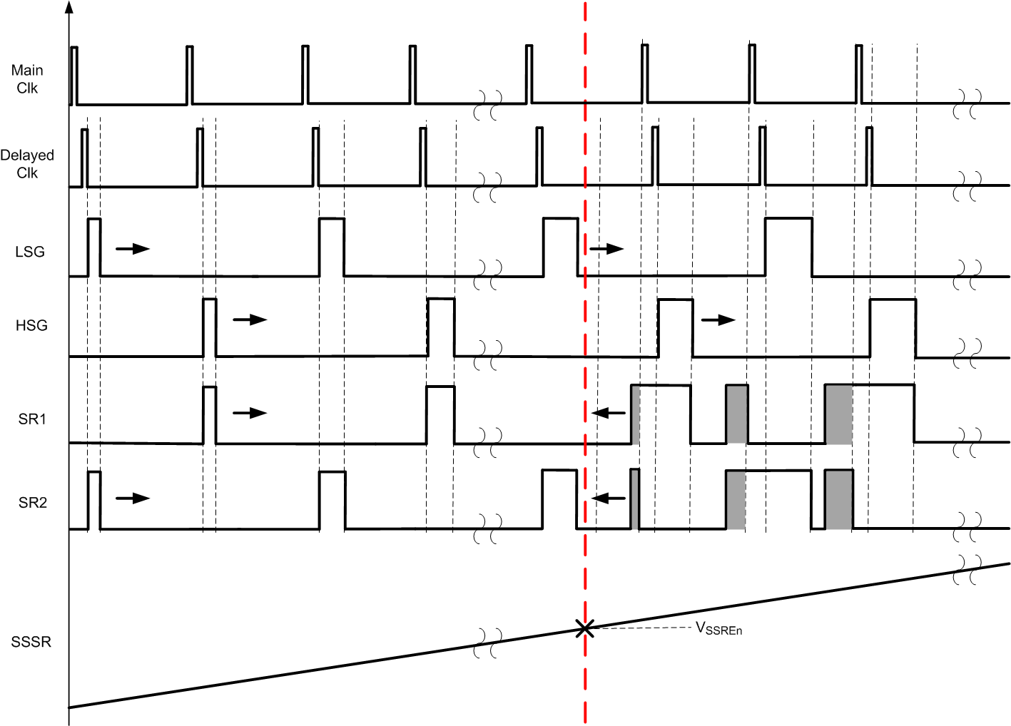
 Figure 7-10 PWM Timing During Startup Process