ZHCSI27C April 2018 – October 2021 LM5036
PRODUCTION DATA
- 1 特性
- 2 应用
- 3 说明
- 4 Revision History
- 5 Pin Configuration and Functions
- 6 Specifications
-
7 Detailed Description
- 7.1 Overview
- 7.2 Functional Block Diagram
- 7.3
Feature Description
- 7.3.1 High-Voltage Start-Up Regulator
- 7.3.2 Undervoltage Lockout (UVLO)
- 7.3.3 Reference Regulator
- 7.3.4 Oscillator, Synchronized Input
- 7.3.5 Voltage-Mode Control
- 7.3.6 Primary-Side Gate Driver Outputs (LSG and HSG)
- 7.3.7 Half-Bridge PWM Scheme
- 7.3.8 Maximum Duty Cycle Operation
- 7.3.9 Pre-Biased Start-Up Process
- 7.3.10 Zero Duty Cycle Operation
- 7.3.11 Enhanced Cycle-by-Cycle Current Limiting with Pulse Matching
- 7.3.12 Reverse Current Protection
- 7.3.13 CBC Threshold Accuracy
- 7.3.14 Hiccup Mode Protection
- 7.3.15 Hiccup Mode Blanking
- 7.3.16 Over-Temperature Protection (OTP)
- 7.3.17 Over-Voltage / Latch (ON_OFF Pin)
- 7.3.18 Auxiliary Constant On-Time Control
- 7.3.19 Auxiliary On-Time Generator
- 7.3.20 Auxiliary Supply Current Limiting
- 7.3.21 Auxiliary Primary Output Capacitor Ripple
- 7.3.22 Auxiliary Ripple Configuration and Control
- 7.3.23 Asynchronous Mode Operation of Auxiliary Supply
- 7.4 Device Functional Modes
-
8 Application and Implementation
- 8.1 Application Information
- 8.2
Typical Application
- 8.2.1 Design Requirements
- 8.2.2
Detailed Design Procedure
- 8.2.2.1 Custom Design With WEBENCH® Tools
- 8.2.2.2 Input Transient Protection
- 8.2.2.3 Level-Shift Detection Circuit
- 8.2.2.4 Applications with VIN > 100-V
- 8.2.2.5 Applications without Pre-Biased Start-Up Requirement
- 8.2.2.6 UVLO Voltage Divider Selection
- 8.2.2.7 Over Voltage, Latch (ON_OFF Pin) Voltage Divider Selection
- 8.2.2.8 SS Capacitor
- 8.2.2.9 SSSR Capacitor
- 8.2.2.10 Half-Bridge Power Stage Design
- 8.2.2.11 Current Limit
- 8.2.2.12 Auxiliary Transformer
- 8.2.2.13 Auxiliary Feedback Resistors
- 8.2.2.14 RON Resistor
- 8.2.2.15 VIN Pin Capacitor
- 8.2.2.16 Auxiliary Primary Output Capacitor
- 8.2.2.17 Auxiliary Secondary Output Capacitor
- 8.2.2.18 Auxiliary Feedback Ripple Circuit
- 8.2.2.19 Auxiliary Secondary Diode
- 8.2.2.20 VCC Diode
- 8.2.2.21 Opto-Coupler Interface
- 8.2.2.22 Full-Bridge Converter Applications
- 8.2.3 Application Curves
- 9 Power Supply Recommendations
- 10Layout
- 11Device and Documentation Support
- 12Mechanical, Packaging, and Orderable Information
7.3.14 Hiccup Mode Protection
A block diagram of the hiccup mode function is shown in Figure 7-17. Both the repetitive CBC and negative current limit events will trigger hiccup mode operation in LM5036 device.
 Figure 7-17 Hiccup Mode Circuitry
The device charges the hiccup restart capacitor with a current source IRES-SRC1 (15-µA typical) during CBC operation. The hiccup mode is activated when VRES exceeds 1 V. During hiccup mode operation, the SS and SSSR capacitors are fully discharged and the half-bridge converter remains off for a period of time (tHIC) before a new soft-start sequence is initiated.
 Figure 7-18 Hiccup Mode Activated By Continuous CBC Operation
Use Equation 26 to calculate the duration of CBC operation before entering the hiccup mode.
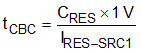
where
- CRES is the value of the hiccup capacitor
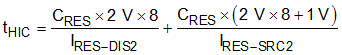
After the RES pin reaches 1.0-V, current source IRES-SRC1 (15-μA typical) is turned off and current source IRES-SRC2 (30-μA typical) is turned on which charges the RES capacitor to 4-V. Then current source IRES-DIS2 (5-μA typical) is enabled which discharges the RES capacitor to 2-V.
Use Equation 27 to calculate the hiccup mode off-time.
In addition to the repetitive CBC current limit condition, the device also enters hiccup mode if the SSSR capacitor is clamped for eight times due to repetitive negative current limit condition. The operating pattern of the hiccup mode activated by the negative current limit is similar to that activated by CBC current limit. The only difference is that at the beginning of the hiccup mode operation the RES capacitor is charged with current source IRES-SRC2 when activated by negative current limit as illustrated in Figure 7-19 whereas the RES capacitor is charged with current source IRES-SRC1 when activated by CBC current limit condition.

Once the hiccup off-timer expires, the SSSR capacitor clamp event counter will be reset. If SSSR capacitor gets clamped for less than eight times before the SSSR capacitor voltage is fully ramped up to its maximum value, the SSSR capacitor clamp event counter will also be reset. This is because the fact that SSSR capacitor voltage is able to fully ramp up to its maximum value indicates that repetitive negative current limit condition no longer exists.