ZHCSA85F August   2012  – February 2019 DLPC410

PRODUCTION DATA.  

  1. 特性
  2. 应用
  3. 说明
    1.     Device Images
      1.      简化应用
  4. 修订历史记录
  5. 说明 (续)
  6. Pin Configuration and Functions
    1.     Pin Functions
  7. Specifications
    1. 7.1 Absolute Maximum Ratings
    2. 7.2 ESD Ratings
    3. 7.3 Recommended Operating Conditions
    4. 7.4 Electrical Characteristics
    5. 7.5 Timing Requirements
  8. Detailed Description
    1. 8.1 Overview
    2. 8.2 Functional Block Diagrams
    3. 8.3 Feature Description
      1. 8.3.1 DLPC410 Binary Pattern Data Path
        1. 8.3.1.1  DIN_A, DIN_B, DIN_C, DIN_D Input Data Buses
        2. 8.3.1.2  DCLKIN Input Clocks
        3. 8.3.1.3  DVALID Input Signals
        4. 8.3.1.4  DOUT_A, DOUT_B, DOUT_C, DOUT_D Output Data Buses
        5. 8.3.1.5  DCLKOUT Output Clocks
        6. 8.3.1.6  SCTRL Output Signals
        7. 8.3.1.7  Supported DMD Bus Sizes
        8. 8.3.1.8  Row Cycle definition
        9. 8.3.1.9  DLP9500 and DLP9500UV Input Data Formatting
        10. 8.3.1.10 DLP7000 and DLP7000UV Input Data Bus
        11. 8.3.1.11 DLP650LNIR Input Data Bus
      2. 8.3.2 Data Bus Operations
        1. 8.3.2.1 Row Addressing
        2. 8.3.2.2 Single Row Write Operation
        3. 8.3.2.3 No-Op Row Cycle Description
      3. 8.3.3 DMD Block Operations
        1. 8.3.3.1 Mirror Clocking Pulse (MCP)
        2. 8.3.3.2 Reset Active (RST_ACTIVE)
        3. 8.3.3.3 DMD Block Control Signals
          1. 8.3.3.3.1 Block Mode - BLK_MD1:0)
          2. 8.3.3.3.2 Block Address - BLK_AD(3:0)
          3. 8.3.3.3.3 Reset 2 Blocks - RST2BLK
        4. 8.3.3.4 DMD Block Operations
          1. 8.3.3.4.1 Global Reset (MCP) Consideration
      4. 8.3.4 Other Data Control Inputs
        1. 8.3.4.1 Complement Data
        2. 8.3.4.2 North/South Flip
      5. 8.3.5 Miscellaneous Control Inputs
        1. 8.3.5.1 ARST
        2. 8.3.5.2 CLKIN_R
        3. 8.3.5.3 DMD_A_RESET
        4. 8.3.5.4 Watchdog Timer Enable (WDT_ENABLE)
      6. 8.3.6 Miscellaneous Status Outputs
        1. 8.3.6.1 INIT_ACTIVE
        2. 8.3.6.2 DMD_Type(3:0)
        3. 8.3.6.3 DDC_VERSION(3:0)
        4. 8.3.6.4 LED0
        5. 8.3.6.5 LED1
        6. 8.3.6.6 DLPA200 Control Signals
        7. 8.3.6.7 ECM2M_TP_ (31:0)
    4. 8.4 Device Functional Modes
      1. 8.4.1 DLPC410 Initialization and Training
        1. 8.4.1.1 Initialization
        2. 8.4.1.2 input Data Interface (DIN) Training Pattern
      2. 8.4.2 DLPC410 Operational Modes
        1. 8.4.2.1 Single Block Mode
        2. 8.4.2.2 Single Block Phased Mode
        3. 8.4.2.3 Dual Block Mode
        4. 8.4.2.4 Quad Block Mode
        5. 8.4.2.5 Global Mode
        6. 8.4.2.6 DMD Park Mode
        7. 8.4.2.7 DMD Idle Mode
      3. 8.4.3 LOAD4 Functionality (enabled with DLPR410A)
        1. 8.4.3.1 Enabling LOAD4
        2. 8.4.3.2 Loading Data with LOAD4
        3. 8.4.3.3 Row Mapping with LOAD4
        4. 8.4.3.4 Using Block Clear with LOAD4
        5. 8.4.3.5 Timing Requirements for LOAD4
        6. 8.4.3.6 Global Binary Pattern Rate increases using LOAD4
        7. 8.4.3.7 Special LOAD4 considerations
    5. 8.5 Programming
  9. Application and Implementation
    1. 9.1 Application Information
      1. 9.1.1 Device Description
    2. 9.2 Typical Application
      1. 9.2.1 Design Requirements
      2. 9.2.2 Detailed Design Procedure
      3. 9.2.3 Application Curves
    3. 9.3 Initialization Setup
      1. 9.3.1 Debugging Guidelines
      2. 9.3.2 Initialization
        1. 9.3.2.1 Calibration
        2. 9.3.2.2 DLPA200 Number 1 Initialization
        3. 9.3.2.3 DMD Initialization
          1. 9.3.2.3.1 DMD Device ID Check
          2. 9.3.2.3.2 DMD Device OK
        4. 9.3.2.4 DLPA200 Number 2 Initialization
        5. 9.3.2.5 Command Sequence Initialization
      3. 9.3.3 Image Display Issues
        1. 9.3.3.1 Present Data to DLPC410
        2. 9.3.3.2 Load Data to DMD
        3. 9.3.3.3 Mirror Clocking Pulse
  10. 10Power Supply Recommendations
    1. 10.1 Power Down Operation
  11. 11Layout
    1. 11.1 Layout Guidelines
      1. 11.1.1 Impedance Requirements
      2. 11.1.2 PCB Signal Routing
      3. 11.1.3 Fiducials
      4. 11.1.4 PCB Layout Guidelines
        1. 11.1.4.1 DMD Interface
          1. 11.1.4.1.1 Trace Length Matching
        2. 11.1.4.2 DLPC410 DMD Decoupling
          1. 11.1.4.2.1 Decoupling Capacitors
        3. 11.1.4.3 VCC and VCC2
        4. 11.1.4.4 DMD Layout
        5. 11.1.4.5 DLPA200
    2. 11.2 Layout Example
    3. 11.3 DLPC410 Chipset Connections
  12. 12器件和文档支持
    1. 12.1 器件支持
      1. 12.1.1 器件标记
      2. 12.1.2 器件命名规则
    2. 12.2 文档支持
      1. 12.2.1 相关文档
    3. 12.3 社区资源
    4. 12.4 商标
    5. 12.5 静电放电警告
    6. 12.6 术语表
  13. 13机械、封装和可订购信息

封装选项

机械数据 (封装 | 引脚)
  • DLP|676
散热焊盘机械数据 (封装 | 引脚)
订购信息

Single Row Write Operation

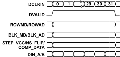
Once initialization is complete (INIT_ACTIVE = 0) the user is free to send data and control information to the DLPC410. When the user asserts the DVALID signal for the LVDS input buses, the DLPC410 samples the customer supplied binary input pattern data (DIN) as well as the Row Mode, Row Address, Block Mode, Block Address, and other control information. The DLPC410 then sends pattern data synchronously to the DMD along with row address and control information. The row cycle period is defined by the Clocks per Row in Table 11 and is synchronous with DVALID as shown in Figure 10. If DVALID is removed midway in a Row Cycle, the DLPC410 continues loading data regardless of data validity until the internal row cycle counter reaches the terminal count of Clocks/Row for that DMD.

Figure 10 is an example of a single Row Cycle for the DLP7000 DMD. A total of 32 bits of input data are presented to the DLPC410 on each clock edge (16 bits on Bus A + 16 bits on Bus B) . An entire line must be written for data to be latched into DMD memory and it requires 16 DDR clock cycles to write a single row of 1024 bits.
DLPC410 sing_write_oper_lps024.gifFigure 10. Single Row Write Operation (DLP7000 DMD)