ZHCSA85F August   2012  – February 2019 DLPC410

PRODUCTION DATA.  

  1. 特性
  2. 应用
  3. 说明
    1.     Device Images
      1.      简化应用
  4. 修订历史记录
  5. 说明 (续)
  6. Pin Configuration and Functions
    1.     Pin Functions
  7. Specifications
    1. 7.1 Absolute Maximum Ratings
    2. 7.2 ESD Ratings
    3. 7.3 Recommended Operating Conditions
    4. 7.4 Electrical Characteristics
    5. 7.5 Timing Requirements
  8. Detailed Description
    1. 8.1 Overview
    2. 8.2 Functional Block Diagrams
    3. 8.3 Feature Description
      1. 8.3.1 DLPC410 Binary Pattern Data Path
        1. 8.3.1.1  DIN_A, DIN_B, DIN_C, DIN_D Input Data Buses
        2. 8.3.1.2  DCLKIN Input Clocks
        3. 8.3.1.3  DVALID Input Signals
        4. 8.3.1.4  DOUT_A, DOUT_B, DOUT_C, DOUT_D Output Data Buses
        5. 8.3.1.5  DCLKOUT Output Clocks
        6. 8.3.1.6  SCTRL Output Signals
        7. 8.3.1.7  Supported DMD Bus Sizes
        8. 8.3.1.8  Row Cycle definition
        9. 8.3.1.9  DLP9500 and DLP9500UV Input Data Formatting
        10. 8.3.1.10 DLP7000 and DLP7000UV Input Data Bus
        11. 8.3.1.11 DLP650LNIR Input Data Bus
      2. 8.3.2 Data Bus Operations
        1. 8.3.2.1 Row Addressing
        2. 8.3.2.2 Single Row Write Operation
        3. 8.3.2.3 No-Op Row Cycle Description
      3. 8.3.3 DMD Block Operations
        1. 8.3.3.1 Mirror Clocking Pulse (MCP)
        2. 8.3.3.2 Reset Active (RST_ACTIVE)
        3. 8.3.3.3 DMD Block Control Signals
          1. 8.3.3.3.1 Block Mode - BLK_MD1:0)
          2. 8.3.3.3.2 Block Address - BLK_AD(3:0)
          3. 8.3.3.3.3 Reset 2 Blocks - RST2BLK
        4. 8.3.3.4 DMD Block Operations
          1. 8.3.3.4.1 Global Reset (MCP) Consideration
      4. 8.3.4 Other Data Control Inputs
        1. 8.3.4.1 Complement Data
        2. 8.3.4.2 North/South Flip
      5. 8.3.5 Miscellaneous Control Inputs
        1. 8.3.5.1 ARST
        2. 8.3.5.2 CLKIN_R
        3. 8.3.5.3 DMD_A_RESET
        4. 8.3.5.4 Watchdog Timer Enable (WDT_ENABLE)
      6. 8.3.6 Miscellaneous Status Outputs
        1. 8.3.6.1 INIT_ACTIVE
        2. 8.3.6.2 DMD_Type(3:0)
        3. 8.3.6.3 DDC_VERSION(3:0)
        4. 8.3.6.4 LED0
        5. 8.3.6.5 LED1
        6. 8.3.6.6 DLPA200 Control Signals
        7. 8.3.6.7 ECM2M_TP_ (31:0)
    4. 8.4 Device Functional Modes
      1. 8.4.1 DLPC410 Initialization and Training
        1. 8.4.1.1 Initialization
        2. 8.4.1.2 input Data Interface (DIN) Training Pattern
      2. 8.4.2 DLPC410 Operational Modes
        1. 8.4.2.1 Single Block Mode
        2. 8.4.2.2 Single Block Phased Mode
        3. 8.4.2.3 Dual Block Mode
        4. 8.4.2.4 Quad Block Mode
        5. 8.4.2.5 Global Mode
        6. 8.4.2.6 DMD Park Mode
        7. 8.4.2.7 DMD Idle Mode
      3. 8.4.3 LOAD4 Functionality (enabled with DLPR410A)
        1. 8.4.3.1 Enabling LOAD4
        2. 8.4.3.2 Loading Data with LOAD4
        3. 8.4.3.3 Row Mapping with LOAD4
        4. 8.4.3.4 Using Block Clear with LOAD4
        5. 8.4.3.5 Timing Requirements for LOAD4
        6. 8.4.3.6 Global Binary Pattern Rate increases using LOAD4
        7. 8.4.3.7 Special LOAD4 considerations
    5. 8.5 Programming
  9. Application and Implementation
    1. 9.1 Application Information
      1. 9.1.1 Device Description
    2. 9.2 Typical Application
      1. 9.2.1 Design Requirements
      2. 9.2.2 Detailed Design Procedure
      3. 9.2.3 Application Curves
    3. 9.3 Initialization Setup
      1. 9.3.1 Debugging Guidelines
      2. 9.3.2 Initialization
        1. 9.3.2.1 Calibration
        2. 9.3.2.2 DLPA200 Number 1 Initialization
        3. 9.3.2.3 DMD Initialization
          1. 9.3.2.3.1 DMD Device ID Check
          2. 9.3.2.3.2 DMD Device OK
        4. 9.3.2.4 DLPA200 Number 2 Initialization
        5. 9.3.2.5 Command Sequence Initialization
      3. 9.3.3 Image Display Issues
        1. 9.3.3.1 Present Data to DLPC410
        2. 9.3.3.2 Load Data to DMD
        3. 9.3.3.3 Mirror Clocking Pulse
  10. 10Power Supply Recommendations
    1. 10.1 Power Down Operation
  11. 11Layout
    1. 11.1 Layout Guidelines
      1. 11.1.1 Impedance Requirements
      2. 11.1.2 PCB Signal Routing
      3. 11.1.3 Fiducials
      4. 11.1.4 PCB Layout Guidelines
        1. 11.1.4.1 DMD Interface
          1. 11.1.4.1.1 Trace Length Matching
        2. 11.1.4.2 DLPC410 DMD Decoupling
          1. 11.1.4.2.1 Decoupling Capacitors
        3. 11.1.4.3 VCC and VCC2
        4. 11.1.4.4 DMD Layout
        5. 11.1.4.5 DLPA200
    2. 11.2 Layout Example
    3. 11.3 DLPC410 Chipset Connections
  12. 12器件和文档支持
    1. 12.1 器件支持
      1. 12.1.1 器件标记
      2. 12.1.2 器件命名规则
    2. 12.2 文档支持
      1. 12.2.1 相关文档
    3. 12.3 社区资源
    4. 12.4 商标
    5. 12.5 静电放电警告
    6. 12.6 术语表
  13. 13机械、封装和可订购信息

封装选项

机械数据 (封装 | 引脚)
  • DLP|676
散热焊盘机械数据 (封装 | 引脚)
订购信息

Timing Requirements

(see (4))
MIN NOM MAX UNIT
fcd Clock frequency, DCLKIN_n(1) 395 400 400 MHz
fcr Clock frequency, CLK_R 50 MHz
tc Cycle time, DCLKIN_n 2.5 2.5 2.53 ns
tw(H) Pulse duration, high 50% to 50% reference points (signal) 1.25 1.25 1.27 ns
tw(L) Pulse duration, low 50% to 50% reference points (signal) 1.25 1.25 1.27 ns
tt Transition time, tt = tf /tr 20% to 80% reference points (signal) .6 ns
tjp Period Jitter DCLKIN_n(2) 150 ps
tSK Skew, DIN_A(15-0) to DCLKIN_A –150 150 ps
Skew, DIN_B(15-0) to DCLKIN_B –150 150
Skew, DIN_C(15-0) to DCLKIN_C –150 150
Skew, DIN_D(15-0) to DCLKIN_D –150 150
Skew, DVALID_n to DCLKIN_n↑ –150 150
Skew, BLK_MD BLK_AD to DCLKIN_n↑(3) –150 150
Skew, ROWMD or ROWAD to DCLKIN_n↑(3) –150 150
Skew, STEPVCC to DCLKIN↑(3) –150 150
Preferred DCLKIN_n duty cycle = 50%
This is the deviation in period from ideal period due solely to high frequency jitter.
First edge of DIN*, ROW*, BLK* and STEPVCC should be synchronous to DVALID rising edge
It is recommended that the COMP_DATA, NS_FLIP and RST2BLK flags be set to one value and not adjusted during normal system operation.
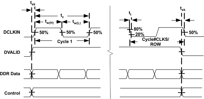
DLPC410 ip_iface_tim_lps024.gifFigure 2. Input Interface Timing
DLPC410 control_tim_lps024.gifFigure 3. Control Timing

NOTE

Dynamic changes to NS_FLIP and COMP_DATA during normal operation is not recommended.