ZHCSA85F August   2012  – February 2019 DLPC410

PRODUCTION DATA.  

  1. 特性
  2. 应用
  3. 说明
    1.     Device Images
      1.      简化应用
  4. 修订历史记录
  5. 说明 (续)
  6. Pin Configuration and Functions
    1.     Pin Functions
  7. Specifications
    1. 7.1 Absolute Maximum Ratings
    2. 7.2 ESD Ratings
    3. 7.3 Recommended Operating Conditions
    4. 7.4 Electrical Characteristics
    5. 7.5 Timing Requirements
  8. Detailed Description
    1. 8.1 Overview
    2. 8.2 Functional Block Diagrams
    3. 8.3 Feature Description
      1. 8.3.1 DLPC410 Binary Pattern Data Path
        1. 8.3.1.1  DIN_A, DIN_B, DIN_C, DIN_D Input Data Buses
        2. 8.3.1.2  DCLKIN Input Clocks
        3. 8.3.1.3  DVALID Input Signals
        4. 8.3.1.4  DOUT_A, DOUT_B, DOUT_C, DOUT_D Output Data Buses
        5. 8.3.1.5  DCLKOUT Output Clocks
        6. 8.3.1.6  SCTRL Output Signals
        7. 8.3.1.7  Supported DMD Bus Sizes
        8. 8.3.1.8  Row Cycle definition
        9. 8.3.1.9  DLP9500 and DLP9500UV Input Data Formatting
        10. 8.3.1.10 DLP7000 and DLP7000UV Input Data Bus
        11. 8.3.1.11 DLP650LNIR Input Data Bus
      2. 8.3.2 Data Bus Operations
        1. 8.3.2.1 Row Addressing
        2. 8.3.2.2 Single Row Write Operation
        3. 8.3.2.3 No-Op Row Cycle Description
      3. 8.3.3 DMD Block Operations
        1. 8.3.3.1 Mirror Clocking Pulse (MCP)
        2. 8.3.3.2 Reset Active (RST_ACTIVE)
        3. 8.3.3.3 DMD Block Control Signals
          1. 8.3.3.3.1 Block Mode - BLK_MD1:0)
          2. 8.3.3.3.2 Block Address - BLK_AD(3:0)
          3. 8.3.3.3.3 Reset 2 Blocks - RST2BLK
        4. 8.3.3.4 DMD Block Operations
          1. 8.3.3.4.1 Global Reset (MCP) Consideration
      4. 8.3.4 Other Data Control Inputs
        1. 8.3.4.1 Complement Data
        2. 8.3.4.2 North/South Flip
      5. 8.3.5 Miscellaneous Control Inputs
        1. 8.3.5.1 ARST
        2. 8.3.5.2 CLKIN_R
        3. 8.3.5.3 DMD_A_RESET
        4. 8.3.5.4 Watchdog Timer Enable (WDT_ENABLE)
      6. 8.3.6 Miscellaneous Status Outputs
        1. 8.3.6.1 INIT_ACTIVE
        2. 8.3.6.2 DMD_Type(3:0)
        3. 8.3.6.3 DDC_VERSION(3:0)
        4. 8.3.6.4 LED0
        5. 8.3.6.5 LED1
        6. 8.3.6.6 DLPA200 Control Signals
        7. 8.3.6.7 ECM2M_TP_ (31:0)
    4. 8.4 Device Functional Modes
      1. 8.4.1 DLPC410 Initialization and Training
        1. 8.4.1.1 Initialization
        2. 8.4.1.2 input Data Interface (DIN) Training Pattern
      2. 8.4.2 DLPC410 Operational Modes
        1. 8.4.2.1 Single Block Mode
        2. 8.4.2.2 Single Block Phased Mode
        3. 8.4.2.3 Dual Block Mode
        4. 8.4.2.4 Quad Block Mode
        5. 8.4.2.5 Global Mode
        6. 8.4.2.6 DMD Park Mode
        7. 8.4.2.7 DMD Idle Mode
      3. 8.4.3 LOAD4 Functionality (enabled with DLPR410A)
        1. 8.4.3.1 Enabling LOAD4
        2. 8.4.3.2 Loading Data with LOAD4
        3. 8.4.3.3 Row Mapping with LOAD4
        4. 8.4.3.4 Using Block Clear with LOAD4
        5. 8.4.3.5 Timing Requirements for LOAD4
        6. 8.4.3.6 Global Binary Pattern Rate increases using LOAD4
        7. 8.4.3.7 Special LOAD4 considerations
    5. 8.5 Programming
  9. Application and Implementation
    1. 9.1 Application Information
      1. 9.1.1 Device Description
    2. 9.2 Typical Application
      1. 9.2.1 Design Requirements
      2. 9.2.2 Detailed Design Procedure
      3. 9.2.3 Application Curves
    3. 9.3 Initialization Setup
      1. 9.3.1 Debugging Guidelines
      2. 9.3.2 Initialization
        1. 9.3.2.1 Calibration
        2. 9.3.2.2 DLPA200 Number 1 Initialization
        3. 9.3.2.3 DMD Initialization
          1. 9.3.2.3.1 DMD Device ID Check
          2. 9.3.2.3.2 DMD Device OK
        4. 9.3.2.4 DLPA200 Number 2 Initialization
        5. 9.3.2.5 Command Sequence Initialization
      3. 9.3.3 Image Display Issues
        1. 9.3.3.1 Present Data to DLPC410
        2. 9.3.3.2 Load Data to DMD
        3. 9.3.3.3 Mirror Clocking Pulse
  10. 10Power Supply Recommendations
    1. 10.1 Power Down Operation
  11. 11Layout
    1. 11.1 Layout Guidelines
      1. 11.1.1 Impedance Requirements
      2. 11.1.2 PCB Signal Routing
      3. 11.1.3 Fiducials
      4. 11.1.4 PCB Layout Guidelines
        1. 11.1.4.1 DMD Interface
          1. 11.1.4.1.1 Trace Length Matching
        2. 11.1.4.2 DLPC410 DMD Decoupling
          1. 11.1.4.2.1 Decoupling Capacitors
        3. 11.1.4.3 VCC and VCC2
        4. 11.1.4.4 DMD Layout
        5. 11.1.4.5 DLPA200
    2. 11.2 Layout Example
    3. 11.3 DLPC410 Chipset Connections
  12. 12器件和文档支持
    1. 12.1 器件支持
      1. 12.1.1 器件标记
      2. 12.1.2 器件命名规则
    2. 12.2 文档支持
      1. 12.2.1 相关文档
    3. 12.3 社区资源
    4. 12.4 商标
    5. 12.5 静电放电警告
    6. 12.6 术语表
  13. 13机械、封装和可订购信息

封装选项

机械数据 (封装 | 引脚)
  • DLP|676
散热焊盘机械数据 (封装 | 引脚)
订购信息

Typical Application

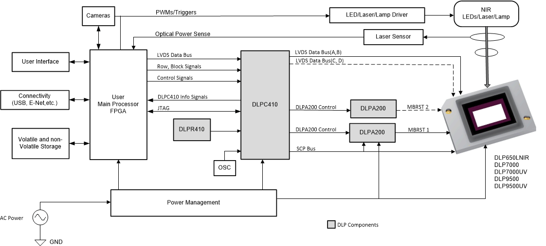
A typical embedded system application using the DLPC410 controller is shown in Figure 22. The DLPC410, the DMD, and their associated DLP components do not specifically determine the application in which the components are used - customer applications and use cases may vary widely, from Digital Image Lithography to 3D Printing to 3D Scanners using Structured Light. The DMD is capable of being used with multiple illumination source types, from Lasers and LEDs to wide band wavelength mercury halide lamps. The DLPC410 supported DMDs cover applications utilizing ultraviolet (UV), visible, and/or near-infrared (NIR) wavelengths. The duration of each binary pattern displayed on the DMD is totally under control of the Applications Processor. The displayed patterns could be strictly binary patterns or could be bit weight exposures of varying durations representing encoded PWM-based gray scales. The timing of the micromirrors and the illumination sources are controlled at the discretion of a Customer Applications Processor and in many solid state cases, provide best performance when source illuminators are synchronous to the commanded DMD micromirror transitions. The speed, diversity, programmability, and flexibility of the DLPC410 building blocks provide an electro-optical cornerstone for customers to build upon to create applications limited only by customer ingenuity.

In Figure 22, the MBRST 2 signals and the C, D LVDS Data buses are shown with dashed lines to indicate that some DMDs do not require these signals to be used. TI's Reference Design and Evaluation Modules leverage a DLPC410 Controller Board which supports all 5 of the DLPC410 supported DMDs. The performance differences for each application are determined by which DMD Board is plugged into the Controller Board. This provides a single DLPC410 design platform which can then be used for multiple customer SKUs within an application platform for product segmentation purposes.
DLPC410 DLPC410_Apps_Block_Diag_all_DMDs.gifFigure 22. DLPC410 Application Example Block Diagram