ZHCSO18A december 2022 – june 2023 TPS281C30
PRODUCTION DATA
- 1
- 1 特性
- 2 应用
- 3 说明
- 4 Revision History
- 5 Device Comparison Table
- 6 Pin Configuration and Functions
- 7 Specifications
- 8 Parameter Measurement Information
- 9 Detailed Description
- 10Application and Implementation
- 11Device and Documentation Support
- 12Mechanical, Packaging, and Orderable Information
9.4.5.5 Reverse Polarity Protection
Method 1: Blocking diode connected with VBB. Both the device and load are protected when in reverse polarity. The blocking diode does not allow any of the current to flow during reverse battery condition.
 Figure 9-17 Reverse Protection With Blocking Diode
Method 2 (GND network protection): Only the high-side device is protected under this connection. The load reverse loop is limited by the load itself. Note when reverse polarity happens, the continuous reverse current through the power FET should be less than Irev. Of the three types of ground pin networks, TI strongly recommends type 3 (the resistor and diode in parallel). No matter what types of connection are between the device GND and the board GND, if a GND voltage shift happens, ensure the following proper connections for the normal operation:
- Leave the NC pin floating or connect to the device GND. TI recommends to leave floating.
- Connect the current limit programmable resistor to the device GND.
 Figure 9-18 Reverse Protection With GND Network
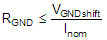
- Type 1 (resistor): The higher resistor value contributes to a better current limit effect when the reverse battery or negative ISO pulses. However, it leads to higher GND shift during normal operation mode. Also, consider the resistor’s power dissipation. Equation 9.
 Equation 10.
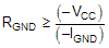
where
- VGNDshift is the maximum value for the GND shift, determined by the HSS and microcontroller. TI suggests a value ≤ 0.6 V.
- Inom is the nominal operating current.
- –VCC is the maximum reverse voltage seen on the battery line.
- –IGND is the maximum reverse current the ground pin can withstand, which is available in the Absolute Maximum Ratings.
If multiple high-side power switches are used, the resistor can be shared among devices.
- Type 2 (diode): A diode is needed to block the reverse voltage, which also brings a ground shift (≈ 600 mV). However, an inductive load is not acceptable to avoid an abnormal status when switching off.
- Type 3 (resistor and diode in parallel (recommended)): A peak negative spike may occur when the inductive load is switching off, which may damage the HSD or the diode. So, TI recommends a resistor in parallel with the diode when driving an inductive load. The recommended selection are 1-kΩ resistor in parallel with an IF > 100-mA diode. If multiple high-side switches are used, the resistor and diode can be shared among devices.