ZHCSO18A december   2022  – june 2023 TPS281C30

PRODUCTION DATA  

  1.   1
  2. 特性
  3. 应用
  4. 说明
  5. Revision History
  6. Device Comparison Table
  7. Pin Configuration and Functions
  8. Specifications
    1. 7.1 Absolute Maximum Ratings
    2. 7.2 ESD Ratings
    3. 7.3 Recommended Operating Conditions
    4. 7.4 Thermal Information
    5. 7.5 Thermal Information
    6. 7.6 Electrical Characteristics
    7. 7.7 SNS Timing Characteristics
    8. 7.8 Switching Characteristics
    9. 7.9 Typical Characteristics
  9. Parameter Measurement Information
  10. Detailed Description
    1. 9.1 Overview
    2. 9.2 Functional Block Diagram
    3. 9.3 Device Functional Modes
      1. 9.3.1 Working Mode
    4. 9.4 Feature Description
      1. 9.4.1 Accurate Current Sense
        1. 9.4.1.1 High Accuracy Sense Mode
      2. 9.4.2 Programmable Current Limit
        1. 9.4.2.1 Short-Circuit and Overload Protection
        2. 9.4.2.2 Capacitive Charging
      3. 9.4.3 Inductive-Load Switching-Off Clamp
      4. 9.4.4 Inductive Load Demagnetization
      5. 9.4.5 Full Protections and Diagnostics
        1. 9.4.5.1 Open-Load Detection
        2. 9.4.5.2 Thermal Protection Behavior
        3. 9.4.5.3 Undervoltage Lockout (UVLO) Protection
        4. 9.4.5.4 Overvoltage (OVP) Protection
        5. 9.4.5.5 Reverse Polarity Protection
        6. 9.4.5.6 Protection for MCU I/Os
        7. 9.4.5.7 Diagnostic Enable Function
        8. 9.4.5.8 Loss of Ground
  11. 10Application and Implementation
    1. 10.1 Application Information
    2. 10.2 Typical Application
      1. 10.2.1 Design Requirements
        1. 10.2.1.1 IEC 61000-4-5 Surge
      2. 10.2.2 Detailed Design Procedure
        1. 10.2.2.1 Selecting RILIM
        2. 10.2.2.2 Selecting RSNS
    3. 10.3 Power Supply Recommendations
    4. 10.4 Layout
      1. 10.4.1 Layout Guidelines
        1. 10.4.1.1 EMC Considerations
      2. 10.4.2 Layout Example
        1. 10.4.2.1 PWP Layout without a GND Network
        2. 10.4.2.2 PWP Layout with a GND Network
        3. 10.4.2.3 RGW Layout with a GND Network
      3. 10.4.3 Thermal Considerations
  12. 11Device and Documentation Support
    1. 11.1 接收文档更新通知
    2. 11.2 支持资源
    3. 11.3 Trademarks
    4. 11.4 静电放电警告
    5. 11.5 术语表
  13. 12Mechanical, Packaging, and Orderable Information

封装选项

机械数据 (封装 | 引脚)
散热焊盘机械数据 (封装 | 引脚)
订购信息

Inductive Load Demagnetization

When switching off an inductive load, the inductor can impose a negative voltage on the output of the switch. The TPS281C30 includes voltage clamps between VS and VOUT to limit the voltage across the FETs and demagnetize load inductance if there is any. The negative voltage applied at the OUT pin drives the discharge of inductor current. Figure 10-14 shows the device discharging a 400-mH load.
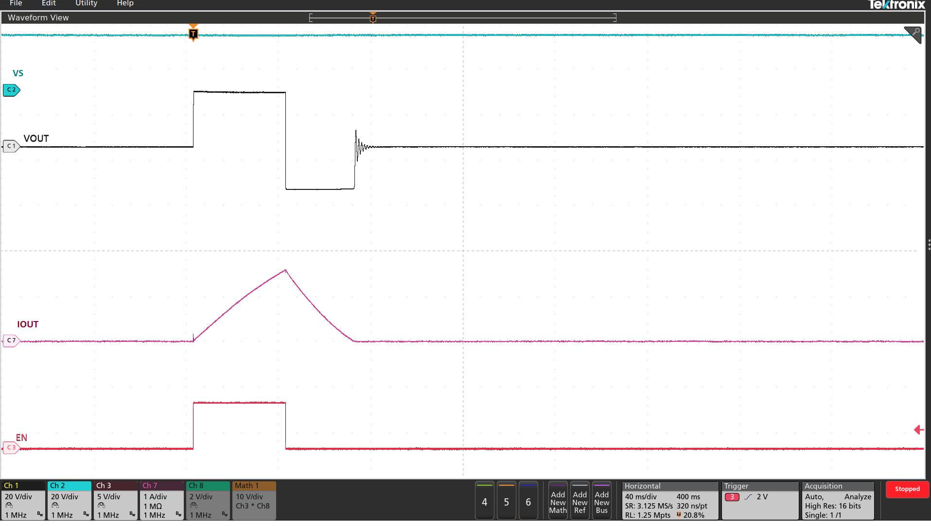
GUID-20221219-SS0I-PXQK-GQ8T-F4RWJSP14LHR-low.pngFigure 9-13 TPS281C30 Inductive Discharge (400 mH).
The maximum acceptable load inductance is a function of the energy dissipated in the device and therefore the load current and the inductive load. The maximum energy and the load inductance the device can withstand for one pulse inductive dissipation at 125°C is shown in Figure 10-15. The device can withstand 50% of this energy for one million inductive repetitive pulses with a >4-Hz repetitive pulse. If the application parameters exceed this device limit, use a protection device like a freewheeling diode to dissipate the energy stored in the inductor.

GUID-20221221-SS0I-8CJT-X3ZF-XWN3LZBRJZHG-low.svgFigure 9-14 TPS281C30 Inductive Load Discharge Energy Capability at 125°C.