ZHCSJK5D January 2018 – June 2022 TCAN4550-Q1
PRODUCTION DATA
- 1 特性
- 2 应用
- 3 说明
- 4 Revision History
- 5 Pin Configuration and Functions
-
6 Specification
- 6.1 Absolute Maximum Ratings
- 6.2 ESD Ratings
- 6.3 ESD Ratings, IEC ESD and ISO Transient Specification
- 6.4 Recommended Operating Conditions
- 6.5 Thermal Information
- 6.6 Supply Characteristics
- 6.7 Electrical Characteristics
- 6.8 Timing Requirements
- 6.9 Switching Characteristics
- 6.10 Typical Characteristics
- 7 Parameter Measurement Information
-
8 Detailed Description
- 8.1 Overview
- 8.2 Functional Block Diagram
- 8.3 Feature Description
- 8.4
Device Functional Modes
- 8.4.1 Normal Mode
- 8.4.2 Standby Mode
- 8.4.3 Sleep Mode
- 8.4.4 Test Mode
- 8.4.5 Failsafe Feature
- 8.4.6 Protection Features
- 8.4.7 CAN FD
- 8.5 Programming
- 8.6
Register Maps
- 8.6.1
Device ID and Interrupt/Diagnostic Flag Registers: 16'h0000 to 16'h002F
- 8.6.1.1 DEVICE_ID1[31:0] (address = h0000) [reset = h4E414354]
- 8.6.1.2 DEVICE_ID2[31:0] (address = h0004) [reset = h30353534]
- 8.6.1.3 Revision (address = h0008) [reset = h00110201]
- 8.6.1.4 Status (address = h000C) [reset = h0000000U]
- 8.6.1.5 SPI Error status mask (address = h0010) [reset = h00000000]
- 8.6.2 Device Configuration Registers: 16'h0800 to 16'h08FF
- 8.6.3 Interrupt/Diagnostic Flag and Enable Flag Registers: 16'h0820/0824 and 16'h0830
- 8.6.4
CAN FD Register Set: 16'h1000 to 16'h10FF
- 8.6.4.1 Core Release Register (address = h1000) [reset = hrrrddddd]
- 8.6.4.2 Endian Register (address = h1004) [reset = h87654321]
- 8.6.4.3 Customer Register (address = h1008) [reset = h00000000]
- 8.6.4.4 Data Bit Timing & Prescaler (address = h100C) [reset = h0000A33]
- 8.6.4.5 Test Register (address = h1010 ) [reset = h00000000]
- 8.6.4.6 RAM Watchdog (address = h1014) [reset = h00000000]
- 8.6.4.7 Control Register (address = h1018) [reset = 0000 0019]
- 8.6.4.8 Nominal Bit Timing & Prescaler Register (address = h101C) [reset = h06000A03]
- 8.6.4.9 Timestamp Counter Configuration (address = h1020) [reset = h00000000]
- 8.6.4.10 Timestamp Counter Value (address = h1024) [reset = h00000000]
- 8.6.4.11 Timeout Counter Configuration (address = h1028) [reset = hFFFF0000]
- 8.6.4.12 Timeout Counter Value (address = h102C) [reset = h0000FFFF]
- 8.6.4.13 Reserved (address = h1030 - h103C) [reset = h00000000]
- 8.6.4.14 Error Counter Register (address = h1040) [reset = h00000000]
- 8.6.4.15 Protocol Status Register (address = h1044) [reset = h00000707]
- 8.6.4.16 Transmitter Delay Compensation Register (address = h1048) [reset = h00000000]
- 8.6.4.17 Reserved (address = h104C) [reset = h00000000]
- 8.6.4.18 Interrupt Register (address = h1050) [reset = h00000000]
- 8.6.4.19 Interrupt Enable (address = h1054) [reset = h00000000]
- 8.6.4.20 Interrupt Line Select (address = h1058) [reset = h00000000]
- 8.6.4.21 Interrupt Line Enable (address = h105C) [reset = h00000000]
- 8.6.4.22 Reserved (address = h1060 - h107C) [reset = h00000000]
- 8.6.4.23 Global Filter Configuration (address = h1080) [reset = h00000000]
- 8.6.4.24 Standard ID Filter Configuration (address = h1084) [reset = h00000000]
- 8.6.4.25 Extended ID Filter Configuration (address = h1088) [reset = h00000000]
- 8.6.4.26 Reserved (address = h108C) [reset = h00000000]
- 8.6.4.27 Extended ID AND Mask (address = h1090) [reset = h1FFFFFFF]
- 8.6.4.28 High Priority Message Status (address = h1094) [reset = h00000000]
- 8.6.4.29 New Data 1 (address = h1098) [reset = h00000000]
- 8.6.4.30 New Data 2 (address = h109C) [reset = h00000000]
- 8.6.4.31 Rx FIFO 0 Configuration (address = h10A0) [reset = h00000000]
- 8.6.4.32 Rx FIFO 0 Status (address = h10A4) [reset = h00000000]
- 8.6.4.33 Rx FIFO 0 Acknowledge (address = h10A8) [reset = h00000000]
- 8.6.4.34 Rx Buffer Configuration (address = h10AC) [reset = h00000000]
- 8.6.4.35 Rx FIFO 1 Configuration (address = h10B0) [reset = h00000000]
- 8.6.4.36 Rx FIFO 1 Status (address = h10B4) [reset = h00000000]
- 8.6.4.37 Rx FIFO 1 Acknowledge (address = h10B8) [reset = h00000000]
- 8.6.4.38 Rx Buffer/FIFO Element Size Configuration (address = h10BC) [reset = h00000000]
- 8.6.4.39 Tx Buffer Configuration (address = h10C0) [reset = h00000000]
- 8.6.4.40 Tx FIFO/Queue Status (address = h10C4) [reset = h00000000]
- 8.6.4.41 Tx Buffer Element Size Configuration (address = h10C8) [reset = h00000000]
- 8.6.4.42 Tx Buffer Request Pending (address = h10CC) [reset = h00000000]
- 8.6.4.43
Tx Buffer Add Request (address = h10D0) [reset = h00000000]
- 8.6.4.43.1 Tx Buffer Cancellation Request (address = h10D4 [reset = h00000000]
- 8.6.4.43.2 Tx Buffer Add Request Transmission Occurred (address = h10D8) [reset = h00000000]
- 8.6.4.43.3 Tx Buffer Cancellation Finished (address = h10DC) [reset = h00000000]
- 8.6.4.43.4 Tx Buffer Transmission Interrupt Enable (address = h10E0) [reset = h00000000]
- 8.6.4.43.5 Tx Buffer Cancellation Finished Interrupt Enable (address = h10E4) [reset = h00000000]
- 8.6.4.43.6 Reserved (address = h10E8) [reset = h00000000]
- 8.6.4.43.7 Reserved (address = h10EC) [reset = h00000000]
- 8.6.4.43.8 Tx Event FIFO Configuration (address = h10F0) [reset = h00000000]
- 8.6.4.43.9 Tx Event FIFO Status (address = h10F4) [reset = h00000000]
- 8.6.4.43.10 Tx Event FIFO Acknowledge (address = h10F8) [reset = h00000000]
- 8.6.4.43.11 Reserved (address = h10FC) [reset = h00000000]
- 8.6.1
Device ID and Interrupt/Diagnostic Flag Registers: 16'h0000 to 16'h002F
- 9 Application and Implementation
- 10Power Supply Recommendations
- 11Layout
- 12Device and Documentation Support
- 13Mechanical, Packaging, and Orderable Information
8.4.5 Failsafe Feature
The TCAN4550-Q1 has three methods the failsafe feature is used in order to reduce node power consumption for a node system issue. Failsafe is the method the device uses to enter sleep mode from various other modes when specific issues arise. This feature uses the Sleep Wake Error (SWE) timer to determine if the node processor can communicate to the TCAN4550-Q1. The SWE timer is default enabled through the SWE_DIS; 16'h0800[1] = 0 but can be disabled by writing a one to this bit. Even when the timer is disabled, a power on reset re-enables the timer and thus be active. Failsafe Feature is default disabled but can be enabled by writing a one to 16'h0800[13], FAILSAFE_EN.
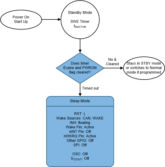
Upon power up, the SWE timer starts, tINACTIVE, the processor has typically four minutes to configure the TCAN4550-Q1, clear the PWRON flag or configure the device for normal mode; see Figure 8-14. This feature cannot be disabled. If the device has not had the PWRON flag cleared or been placed into normal mode, it enters sleep mode. The device wakes up if the CAN bus provides a WUP or a local wake event takes place, thus entering standby mode. Once in standby mode, tSILENCE and tINACTIVE timers starts. If tINACTIVE expires, the device re-enters sleep mode.
The second failure mechanism that causes the device to use the failsafe feature, if enabled, is when the device receives a CANINT, CAN bus wake (WUP) or WAKE pin (LWU), while in sleep mode such that the device leaves sleep mode and enters standby mode. The processor has four minutes to clear the flags and place the device into normal mode. If this does not happen the device enters sleep mode.
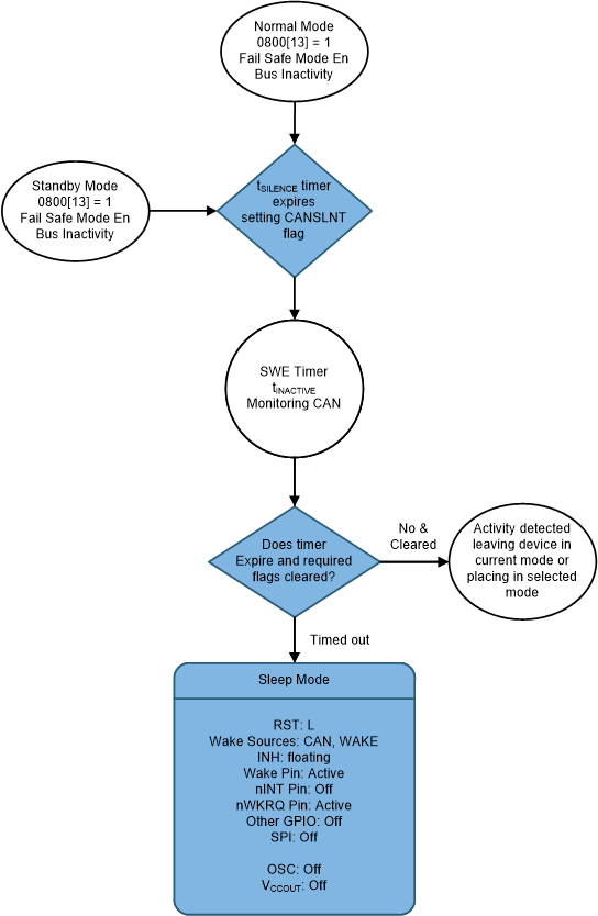
The third failure mechanism that causes the device to use the failsafe feature is when in standby or normal mode and the CANSLNT flag persists for tINACTIVE, the device enters sleep mode. Examples of events that could create this are CLKIN or Crystal stops working, processor is no longer working and not able to exercise the SPI bus, a go-to-sleep command comes in and the processor is not able to receive it or is not able to respond. See state diagram Figure 8-15.
 Figure 8-14 Power On Failsafe Feature
 Figure 8-15 Normal and Standby Failsafe Feature