ZHCSK66C January 2014 – August 2019 ADS1283
PRODUCTION DATA.
- 1 特性
- 2 应用
- 3 说明
- 4 修订历史记录
- 5 Pin Configuration and Functions
- 6 Specifications
- 7 Parameter Measurement Information
-
8 Detailed Description
- 8.1 Overview
- 8.2 Functional Block Diagram
- 8.3 Feature Description
- 8.4
Device Functional Modes
- 8.4.1 Synchronization (SYNC PIN and SYNC Command)
- 8.4.2 Reset (RESET Pin and Reset Command)
- 8.4.3 Power-Down (PWDN Pin and STANDBY Command)
- 8.4.4 Power-On Sequence
- 8.4.5 DVDD Power Supply
- 8.4.6 Serial Interface
- 8.4.7 Data Format
- 8.4.8 Reading Data
- 8.4.9 One-Shot Operation
- 8.4.10 Offset and Full-Scale Calibration Registers
- 8.4.11 Calibration Commands (OFSCAL and GANCAL)
- 8.4.12 User Calibration
- 8.5
Programming
- 8.5.1
Commands
- 8.5.1.1 SDATAC Requirements
- 8.5.1.2 WAKEUP: Wake-Up From Standby Mode
- 8.5.1.3 STANDBY: Standby Mode
- 8.5.1.4 SYNC: Synchronize the Analog-to-Digital Conversion
- 8.5.1.5 RESET: Reset the Device
- 8.5.1.6 RDATAC: Read Data Continuous
- 8.5.1.7 SDATAC: Stop Read Data Continuous
- 8.5.1.8 RDATA: Read Data by Command
- 8.5.1.9 RREG: Read Register Data
- 8.5.1.10 WREG: Write to Register
- 8.5.1.11 OFSCAL: Offset Calibration
- 8.5.1.12 GANCAL: Gain Calibration
- 8.5.1
Commands
- 8.6
Register Maps
- 8.6.1
Register Descriptions
- 8.6.1.1 ID_CFG: ID_Configuration Register (address = 00h) [reset =x0h]
- 8.6.1.2 CONFIG0: Configuration Register 0 (address = 01h) [reset = 52h]
- 8.6.1.3 CONFIG1: Configuration Register 1 (address = 02h) [reset = 08h]
- 8.6.1.4 HPF0 and HPF1 Registers
- 8.6.1.5 OFC0, OFC1, OFC2 Registers
- 8.6.1.6 FSC0, FSC1, FSC2 Registers
- 8.6.1
Register Descriptions
- 9 Application and Implementation
- 10器件和文档支持
- 11机械、封装和可订购信息
8.5.1 Commands
The commands listed in Table 23 control the operation of the ADS1283. Most commands are stand-alone (that is, one byte in length); the register read and write commands are two bytes long in addition to the actual register data bytes.
Table 23. Command Descriptions
| COMMAND | TYPE | DESCRIPTION | 1st COMMAND BYTE(1)(2) | 2nd COMMAND BYTE(3) |
|---|---|---|---|---|
| WAKEUP | Control | Wake-up from standby mode | 0000 000X (00h or 01h) | |
| STANDBY | Control | Enter standby mode | 0000 001X (02h or 03h) | |
| SYNC | Control | Synchronize the analog-to-digital conversion | 0000 010X (04h or 5h) | |
| RESET | Control | Reset registers to default values | 0000 011X (06h or 07h) | |
| RDATAC | Control | Enter read data continuous mode | 0001 0000 (10h) | |
| SDATAC | Control | Stop read data continuous mode | 0001 0001 (11h) | |
| RDATA | Data | Read data by command(4) | 0001 0010 (12h) | |
| RREG | Register | Read nnnnn register(s) at address rrrrr(4) | 001r rrrr (20h + 000r rrrr) | 000n nnnn (00h + n nnnn) |
| WREG | Register | Write nnnnn register(s) at address rrrrr | 010r rrrr (40h + 000r rrrr) | 000n nnnn (00h + n nnnn) |
| OFSCAL | Calibration | Offset calibration | 0110 0000 (60h) | |
| GANCAL | Calibration | Gain calibration | 0110 0001 (61h) |
(1) X = don't care.
(2) rrrrr = starting address for register read and write commands.
(3) nnnnn = number of registers to be read from or written to – 1. For example, to read from or write to three registers, set nnnnn = 2 (00010).
(4) Required to cancel read-data-continuous mode before sending a command.
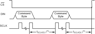
CS must remain low for duration of the command-byte sequence. A delay of 24 fCLK cycles between commands and between bytes within a command is required, starting from the last SCLK rising edge of one command to the first SCLK rising edge of the following command. The required delay is shown in Figure 58.

1. tSCLKDLY = 24 / fCLK (min).
Figure 58. Consecutive Commands