ZHCSK66C January 2014 – August 2019 ADS1283
PRODUCTION DATA.
- 1 特性
- 2 应用
- 3 说明
- 4 修订历史记录
- 5 Pin Configuration and Functions
- 6 Specifications
- 7 Parameter Measurement Information
-
8 Detailed Description
- 8.1 Overview
- 8.2 Functional Block Diagram
- 8.3 Feature Description
- 8.4
Device Functional Modes
- 8.4.1 Synchronization (SYNC PIN and SYNC Command)
- 8.4.2 Reset (RESET Pin and Reset Command)
- 8.4.3 Power-Down (PWDN Pin and STANDBY Command)
- 8.4.4 Power-On Sequence
- 8.4.5 DVDD Power Supply
- 8.4.6 Serial Interface
- 8.4.7 Data Format
- 8.4.8 Reading Data
- 8.4.9 One-Shot Operation
- 8.4.10 Offset and Full-Scale Calibration Registers
- 8.4.11 Calibration Commands (OFSCAL and GANCAL)
- 8.4.12 User Calibration
- 8.5
Programming
- 8.5.1
Commands
- 8.5.1.1 SDATAC Requirements
- 8.5.1.2 WAKEUP: Wake-Up From Standby Mode
- 8.5.1.3 STANDBY: Standby Mode
- 8.5.1.4 SYNC: Synchronize the Analog-to-Digital Conversion
- 8.5.1.5 RESET: Reset the Device
- 8.5.1.6 RDATAC: Read Data Continuous
- 8.5.1.7 SDATAC: Stop Read Data Continuous
- 8.5.1.8 RDATA: Read Data by Command
- 8.5.1.9 RREG: Read Register Data
- 8.5.1.10 WREG: Write to Register
- 8.5.1.11 OFSCAL: Offset Calibration
- 8.5.1.12 GANCAL: Gain Calibration
- 8.5.1
Commands
- 8.6
Register Maps
- 8.6.1
Register Descriptions
- 8.6.1.1 ID_CFG: ID_Configuration Register (address = 00h) [reset =x0h]
- 8.6.1.2 CONFIG0: Configuration Register 0 (address = 01h) [reset = 52h]
- 8.6.1.3 CONFIG1: Configuration Register 1 (address = 02h) [reset = 08h]
- 8.6.1.4 HPF0 and HPF1 Registers
- 8.6.1.5 OFC0, OFC1, OFC2 Registers
- 8.6.1.6 FSC0, FSC1, FSC2 Registers
- 8.6.1
Register Descriptions
- 9 Application and Implementation
- 10器件和文档支持
- 11机械、封装和可订购信息
8.4.3 Power-Down (PWDN Pin and STANDBY Command)
There are two ways to power-down the ADS1283: take the PWDN pin low, or send a STANDBY command. When the PWDN pin is pulled low, the internal circuitry is disabled to minimize power and the contents of the register settings are reset.
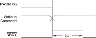
When in a power-down state, the device outputs remain active and the device inputs must not float. When the STANDBY command is sent, the SPI port and the configuration registers are kept active. Figure 48 and Table 15 show the timing. Standby mode is cancelled when CS is taken high.
 Figure 48. PWDN Pin and Wake-Up Command Timing
(Table 15 shows tDR)
Table 15. Power-On, PWDN Pin, and Wake-Up Command Timing for New Data
| PARAMETER | FILTER MODE | ||
|---|---|---|---|
| tDR | Time for data ready 216 CLK cycles after power-on;
and new data ready after PWDN pin or WAKEUP command |
See Table 13 | SINC(1) |
| 62.98046875 / fDATA + 468 / fCLK(2) | FIR | ||
(1) Supply power-on and PWDN pin default is 1000 SPS FIR.
(2) Subtract two CLK cycles for the WAKEUP command. The WAKEUP command is timed from the next rising edge of CLK to after the eighth rising edge of SCLK during command to DRDY falling.