ZHCSK66C January 2014 – August 2019 ADS1283
PRODUCTION DATA.
- 1 特性
- 2 应用
- 3 说明
- 4 修订历史记录
- 5 Pin Configuration and Functions
- 6 Specifications
- 7 Parameter Measurement Information
-
8 Detailed Description
- 8.1 Overview
- 8.2 Functional Block Diagram
- 8.3 Feature Description
- 8.4
Device Functional Modes
- 8.4.1 Synchronization (SYNC PIN and SYNC Command)
- 8.4.2 Reset (RESET Pin and Reset Command)
- 8.4.3 Power-Down (PWDN Pin and STANDBY Command)
- 8.4.4 Power-On Sequence
- 8.4.5 DVDD Power Supply
- 8.4.6 Serial Interface
- 8.4.7 Data Format
- 8.4.8 Reading Data
- 8.4.9 One-Shot Operation
- 8.4.10 Offset and Full-Scale Calibration Registers
- 8.4.11 Calibration Commands (OFSCAL and GANCAL)
- 8.4.12 User Calibration
- 8.5
Programming
- 8.5.1
Commands
- 8.5.1.1 SDATAC Requirements
- 8.5.1.2 WAKEUP: Wake-Up From Standby Mode
- 8.5.1.3 STANDBY: Standby Mode
- 8.5.1.4 SYNC: Synchronize the Analog-to-Digital Conversion
- 8.5.1.5 RESET: Reset the Device
- 8.5.1.6 RDATAC: Read Data Continuous
- 8.5.1.7 SDATAC: Stop Read Data Continuous
- 8.5.1.8 RDATA: Read Data by Command
- 8.5.1.9 RREG: Read Register Data
- 8.5.1.10 WREG: Write to Register
- 8.5.1.11 OFSCAL: Offset Calibration
- 8.5.1.12 GANCAL: Gain Calibration
- 8.5.1
Commands
- 8.6
Register Maps
- 8.6.1
Register Descriptions
- 8.6.1.1 ID_CFG: ID_Configuration Register (address = 00h) [reset =x0h]
- 8.6.1.2 CONFIG0: Configuration Register 0 (address = 01h) [reset = 52h]
- 8.6.1.3 CONFIG1: Configuration Register 1 (address = 02h) [reset = 08h]
- 8.6.1.4 HPF0 and HPF1 Registers
- 8.6.1.5 OFC0, OFC1, OFC2 Registers
- 8.6.1.6 FSC0, FSC1, FSC2 Registers
- 8.6.1
Register Descriptions
- 9 Application and Implementation
- 10器件和文档支持
- 11机械、封装和可订购信息
8.3.3.2.2 FIR Stage
The second stage of the ADS1283 digital filter is an FIR low-pass filter. Data are supplied to this stage from the sinc filter. The FIR stage is segmented into four substages, as shown in Figure 38.
 Figure 38. FIR Filter Substages
 The first two substages are half-band filters with decimation ratios of two. The third substage decimates by four, and the fourth substage decimates by two. The overall decimation of the FIR stage is 32. Note that two coefficient sets are used for the third and fourth sections, depending on the phase selection. Table 8 lists the data rates and overall decimation ratio of the FIR stage. See Table 9 for the FIR filter coefficients.
Table 8. FIR Filter Data Rates
| DR[2:0] REGISTER | DECIMATION RATIO (N) | FIR DATA RATE (SPS) |
|---|---|---|
| 000 | 4096 | 250 |
| 001 | 2048 | 500 |
| 010 | 1024 | 1000 |
| 011 | 512 | 2000 |
| 100 | 256 | 4000 |
Table 9. FIR Stage Coefficients
| COEFFICIENT | SECTION 1 | SECTION 2 | SECTION 3 | SECTION 4 | ||
|---|---|---|---|---|---|---|
| LINEAR PHASE
SCALING = 1 / 512 |
LINEAR PHASE
SCALING = 1 / 8388608 |
SCALING = 1 / 134217728 | SCALING = 1 / 134217728 | |||
| LINEAR
PHASE |
MINIMUM
PHASE |
LINEAR
PHASE |
MINIMUM
PHASE |
|||
| b0 | 3 | –10944 | 0 | 819 | –132 | 11767 |
| b1 | 0 | 0 | 0 | 8211 | –432 | 133882 |
| b2 | –25 | 103807 | –73 | 44880 | –75 | 769961 |
| b3 | 0 | 0 | –874 | 174712 | 2481 | 2940447 |
| b4 | 150 | –507903 | –4648 | 536821 | 6692 | 8262605 |
| b5 | 256 | 0 | –16147 | 1372637 | 7419 | 17902757 |
| b6 | 150 | 2512192 | –41280 | 3012996 | –266 | 30428735 |
| b7 | 0 | 4194304 | –80934 | 5788605 | –10663 | 40215494 |
| b8 | –25 | 2512192 | –120064 | 9852286 | –8280 | 39260213 |
| b9 | 0 | 0 | –118690 | 14957445 | 10620 | 23325925 |
| b10 | 3 | –507903 | –18203 | 20301435 | 22008 | –1757787 |
| b11 | 0 | 224751 | 24569234 | 348 | –21028126 | |
| b12 | 103807 | 580196 | 26260385 | –34123 | –21293602 | |
| b13 | 0 | 893263 | 24247577 | –25549 | –3886901 | |
| b14 | –10944 | 891396 | 18356231 | 33460 | 14396783 | |
| b15 | 293598 | 9668991 | 61387 | 16314388 | ||
| b16 | –987253 | 327749 | –7546 | 1518875 | ||
| b17 | –2635779 | –7171917 | –94192 | –12979500 | ||
| b18 | –3860322 | –10926627 | –50629 | –11506007 | ||
| b19 | –3572512 | –10379094 | 101135 | 2769794 | ||
| b20 | –822573 | –6505618 | 134826 | 12195551 | ||
| b21 | 4669054 | –1333678 | –56626 | 6103823 | ||
| b22 | 12153698 | 2972773 | –220104 | –6709466 | ||
| b23 | 19911100 | 5006366 | –56082 | –9882714 | ||
| b24 | 25779390 | 4566808 | 263758 | –353347 | ||
| b25 | 27966862 | 2505652 | 231231 | 8629331 | ||
| b26 | 25779390 | 126331 | –215231 | 5597927 | ||
| b27 | 19911100 | –1496514 | –430178 | –4389168 | ||
| b28 | 12153698 | –1933830 | 34715 | –7594158 | ||
| b29 | 4669054 | –1410695 | 580424 | –428064 | ||
| b30 | –822573 | –502731 | 283878 | 6566217 | ||
| b31 | –3572512 | 245330 | –588382 | 4024593 | ||
| b32 | –3860322 | 565174 | –693209 | –3679749 | ||
| b33 | –2635779 | 492084 | 366118 | –5572954 | ||
| b34 | –987253 | 231656 | 1084786 | 332589 | ||
| b35 | 293598 | –9196 | 132893 | 5136333 | ||
| b36 | 891396 | –125456 | –1300087 | 2351253 | ||
| b37 | 893263 | –122207 | –878642 | –3357202 | ||
| b38 | 580196 | –61813 | 1162189 | –3767666 | ||
| b39 | 224751 | –4445 | 1741565 | 1087392 | ||
| b40 | –18203 | 22484 | –522533 | 3847821 | ||
| b41 | –118690 | 22245 | –2490395 | 919792 | ||
| b42 | –120064 | 10775 | –688945 | –2918303 | ||
| b43 | –80934 | 940 | 2811738 | –2193542 | ||
| b44 | –41280 | –2953 | 2425494 | 1493873 | ||
| b45 | –16147 | –2599 | –2338095 | 2595051 | ||
| b46 | –4648 | –1052 | –4511116 | –79991 | ||
| b47 | –874 | –43 | 641555 | –2260106 | ||
| b48 | –73 | 214 | 6661730 | –963855 | ||
| b49 | 0 | 132 | 2950811 | 1482337 | ||
| b50 | 0 | 33 | –8538057 | 1480417 | ||
| b51 | 0 | 0 | –10537298 | –586408 | ||
| b52 | 9818477 | –1497356 | ||||
| b53 | 41426374 | –168417 | ||||
| b54 | 56835776 | 1166800 | ||||
| b55 | 41426374 | 644405 | ||||
| b56 | 9818477 | –675082 | ||||
| b57 | –10537298 | –806095 | ||||
| b58 | –8538057 | 211391 | ||||
| b59 | 2950811 | 740896 | ||||
| b60 | 6661730 | 141976 | ||||
| b61 | 641555 | –527673 | ||||
| b62 | –4511116 | –327618 | ||||
| b63 | –2338095 | 278227 | ||||
| b64 | 2425494 | 363809 | ||||
| b65 | 2811738 | –70646 | ||||
| b66 | –688945 | –304819 | ||||
| b67 | –2490395 | –63159 | ||||
| b68 | –522533 | 205798 | ||||
| b69 | 1741565 | 124363 | ||||
| b70 | 1162189 | –107173 | ||||
| b71 | –878642 | –131357 | ||||
| b72 | –1300087 | 31104 | ||||
| b73 | 132893 | 107182 | ||||
| b74 | 1084786 | 15644 | ||||
| b75 | 366118 | –71728 | ||||
| b76 | –693209 | –36319 | ||||
| b77 | –588382 | 38331 | ||||
| b78 | 283878 | 38783 | ||||
| b79 | 580424 | –13557 | ||||
| b80 | 34715 | –31453 | ||||
| b81 | –430178 | –1230 | ||||
| b82 | –215231 | 20983 | ||||
| b83 | 231231 | 7729 | ||||
| b84 | 263758 | –11463 | ||||
| b85 | –56082 | –8791 | ||||
| b86 | –220104 | 4659 | ||||
| b87 | –56626 | 7126 | ||||
| b88 | 134826 | –732 | ||||
| b89 | 101135 | –4687 | ||||
| b90 | –50629 | –976 | ||||
| b91 | –94192 | 2551 | ||||
| b92 | –7546 | 1339 | ||||
| b93 | 61387 | –1103 | ||||
| b94 | 33460 | –1085 | ||||
| b95 | –25549 | 314 | ||||
| b96 | –34123 | 681 | ||||
| b97 | 348 | 16 | ||||
| b98 | 22008 | –349 | ||||
| b99 | 10620 | –96 | ||||
| b100 | –8280 | 144 | ||||
| b101 | –10663 | 78 | ||||
| b102 | –266 | –46 | ||||
| b103 | 7419 | –42 | ||||
| b104 | 6692 | 9 | ||||
| b105 | 2481 | 16 | ||||
| b106 | –75 | 0 | ||||
| b107 | –432 | –4 | ||||
| b108 | –132 | 0 | ||||
| b109 | 0 | 0 | ||||
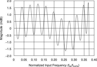
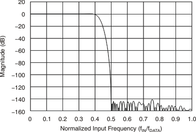
As shown in Figure 39, the FIR frequency response provides a flat pass band to 0.375 of the data rate (±0.003 dB pass-band ripple). Figure 40 shows the transition from pass band to stop band.
 Figure 39. FIR Pass-Band Magnitude Response (fDATA = 500 Hz)
  Figure 40. FIR Transition Band Magnitude Response
 Although not shown in Figure 40, the pass-band response repeats at multiples of the modulator frequency (NfMOD – f0 and NfMOD + f0, where N = 1, 2, and so on, and f0 = pass band). These image frequencies, if present in the signal and not externally filtered, fold back (or alias) into the pass band and cause errors. A low-pass signal filter reduces the effect of aliasing. Often, the RC low-pass filter provided by the PGA output resistors and the external capacitor connected to CAPP and CAPN provide sufficient signal attenuation.