ZHCSK66C January   2014  – August 2019 ADS1283

PRODUCTION DATA.  

  1. 特性
  2. 应用
    1.     简化电路原理图
  3. 说明
  4. 修订历史记录
  5. Pin Configuration and Functions
    1.     Pin Functions
  6. Specifications
    1. 6.1 Absolute Maximum Ratings
    2. 6.2 ESD Ratings
    3. 6.3 Recommended Operating Conditions
    4. 6.4 Thermal Information
    5. 6.5 Electrical Characteristics
    6. 6.6 Timing Requirements
    7. 6.7 Switching Characteristics
    8. 6.8 Typical Characteristics
  7. Parameter Measurement Information
    1. 7.1 Noise Performance
  8. Detailed Description
    1. 8.1 Overview
    2. 8.2 Functional Block Diagram
    3. 8.3 Feature Description
      1. 8.3.1 Analog Inputs and Multiplexer
      2. 8.3.2 Programmable Gain Amplifier (PGA)
      3. 8.3.3 Analog-to-Digital Converter (ADC)
        1. 8.3.3.1 Modulator
          1. 8.3.3.1.1 Modulator Overrange
          2. 8.3.3.1.2 Modulator Input Impedance
          3. 8.3.3.1.3 Modulator Overrange Detection (MFLAG)
          4. 8.3.3.1.4 Offset
          5. 8.3.3.1.5 Voltage Reference Inputs (VREFP, VREFN)
        2. 8.3.3.2 Digital Filter
          1. 8.3.3.2.1 Sinc Filter Stage (sinx / x)
          2. 8.3.3.2.2 FIR Stage
          3. 8.3.3.2.3 Group Delay and Step Response
            1. 8.3.3.2.3.1 Linear Phase Response
            2. 8.3.3.2.3.2 Minimum Phase Response
          4. 8.3.3.2.4 HPF Stage
      4. 8.3.4 Master Clock Input (CLK)
    4. 8.4 Device Functional Modes
      1. 8.4.1  Synchronization (SYNC PIN and SYNC Command)
        1. 8.4.1.1 Pulse-Sync Mode
        2. 8.4.1.2 Continuous-Sync Mode
      2. 8.4.2  Reset (RESET Pin and Reset Command)
      3. 8.4.3  Power-Down (PWDN Pin and STANDBY Command)
      4. 8.4.4  Power-On Sequence
      5. 8.4.5  DVDD Power Supply
      6. 8.4.6  Serial Interface
        1. 8.4.6.1 Chip Select (CS)
        2. 8.4.6.2 Serial Clock (SCLK)
        3. 8.4.6.3 Data Input (DIN)
        4. 8.4.6.4 Data Output (DOUT)
        5. 8.4.6.5 Serial Port Auto Timeout
        6. 8.4.6.6 Data Ready (DRDY)
      7. 8.4.7  Data Format
      8. 8.4.8  Reading Data
        1. 8.4.8.1 Read-Data-Continuous Mode
        2. 8.4.8.2 Read-Data-By-Command Mode
      9. 8.4.9  One-Shot Operation
      10. 8.4.10 Offset and Full-Scale Calibration Registers
        1. 8.4.10.1 OFC[2:0] Registers
        2. 8.4.10.2 FSC[2:0] Registers
      11. 8.4.11 Calibration Commands (OFSCAL and GANCAL)
        1. 8.4.11.1 OFSCAL Command
        2. 8.4.11.2 GANCAL Command
      12. 8.4.12 User Calibration
    5. 8.5 Programming
      1. 8.5.1 Commands
        1. 8.5.1.1  SDATAC Requirements
        2. 8.5.1.2  WAKEUP: Wake-Up From Standby Mode
        3. 8.5.1.3  STANDBY: Standby Mode
        4. 8.5.1.4  SYNC: Synchronize the Analog-to-Digital Conversion
        5. 8.5.1.5  RESET: Reset the Device
        6. 8.5.1.6  RDATAC: Read Data Continuous
        7. 8.5.1.7  SDATAC: Stop Read Data Continuous
        8. 8.5.1.8  RDATA: Read Data by Command
        9. 8.5.1.9  RREG: Read Register Data
        10. 8.5.1.10 WREG: Write to Register
        11. 8.5.1.11 OFSCAL: Offset Calibration
        12. 8.5.1.12 GANCAL: Gain Calibration
    6. 8.6 Register Maps
      1. 8.6.1 Register Descriptions
        1. 8.6.1.1 ID_CFG: ID_Configuration Register (address = 00h) [reset =x0h]
        2. 8.6.1.2 CONFIG0: Configuration Register 0 (address = 01h) [reset = 52h]
        3. 8.6.1.3 CONFIG1: Configuration Register 1 (address = 02h) [reset = 08h]
        4. 8.6.1.4 HPF0 and HPF1 Registers
          1. 8.6.1.4.1 HPF0: High-Pass Filter Corner Frequency, Low Byte (address = 03h) [reset = 32h]
          2. 8.6.1.4.2 HPF1: High-Pass Filter Corner Frequency, High Byte (address = 04h) [reset = 03h]
        5. 8.6.1.5 OFC0, OFC1, OFC2 Registers
          1. 8.6.1.5.1 OFC0: Offset Calibration, Low Byte (address = 05h) [reset = 00h]
          2. 8.6.1.5.2 OFC1: Offset Calibration, Mid Byte (address = 06h) [reset = 00h]
          3. 8.6.1.5.3 OFC2: Offset Calibration, High Byte (address = 07h) [reset = 00h]
        6. 8.6.1.6 FSC0, FSC1, FSC2 Registers
          1. 8.6.1.6.1 FSC0: Full-Scale Calibration, Low Byte (address = 08h) [reset = 00h]
          2. 8.6.1.6.2 FSC1: Full-Scale Calibration, Mid Byte (address = 09h) [reset = 00h]
          3. 8.6.1.6.3 FSC2: Full-Scale Calibration, High Byte (address = 0Ah) [reset = 40h]
  9. Application and Implementation
    1. 9.1 Application Information
    2. 9.2 Typical Applications
      1. 9.2.1 Geophone Interface
      2. 9.2.2 Digital Interface
    3. 9.3 Initialization Set Up
  10. 10器件和文档支持
    1. 10.1 接收文档更新通知
    2. 10.2 社区资源
    3. 10.3 商标
    4. 10.4 静电放电警告
    5. 10.5 Glossary
  11. 11机械、封装和可订购信息

封装选项

机械数据 (封装 | 引脚)
散热焊盘机械数据 (封装 | 引脚)
订购信息

Pulse-Sync Mode

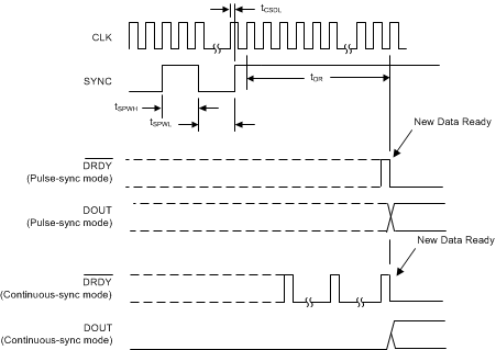
In pulse-sync mode, when a synchronization occurs (by pin or command), the ADS1283 unconditionally stops and restarts the conversion process. When the ADC synchronizes, the device resets the internal filter memory, DRDY goes high, and after the digital filter has settled, new conversion data are available as shown in Figure 45 and Table 12.

ADS1283 ai_tim_sync_sbas565.gifFigure 45. Pulse-Sync and Continuous-Sync Timing With Single Synchronization

Table 12. Pulse-Sync Timing for Figure 45 and Figure 46

PARAMETER MIN MAX UNIT
tCSDL CLK rising edge to SYNC rising edge(2) 30 –30 ns
tSYNC SYNC clock period(1) 1 Infinite n / fDATA
tSPWH, L SYNC pulse width, high or low 2 1 / fCLK
tDR Time for data ready (SINC filter) See Table 13
Time for data ready (FIR filter) 62.98046875 / fDATA + 468 / fCLK
Continuous-sync mode; a free-running clock applied to the SYNC input without causing resynchronization. See Figure 46
CLK rising edge to SYNC rising edge timing must not occur within the specified time window.

Table 13. tDR Time for Data Ready (Sinc Filter)

fDATA (kSPS) fCLK CYCLES(1)
128 440
64 616
32 968
16 1672
8 2824
For SYNC and WAKEUP commands, number of fCLK cycles from next rising CLK edge directly after eighth rising SCLK edge to DRDY falling edge. For WAKEUP command only, subtract two fCLK cycles.

Table 13 is referenced by Table 12 and Table 15.

Observe the timing restriction of SYNC rising edge to CLK rising edge as shown in Figure 45 and Table 12. Synchronization occurs on the next rising CLK edge after the rising edge of the SYNC, or after the eighth rising SCLK edge when synchronized by command. To synchronize multiple ADCs, broadcast the command to the ADCs simultaneously.