ZHCSK66C January   2014  – August 2019 ADS1283

PRODUCTION DATA.  

  1. 特性
  2. 应用
    1.     简化电路原理图
  3. 说明
  4. 修订历史记录
  5. Pin Configuration and Functions
    1.     Pin Functions
  6. Specifications
    1. 6.1 Absolute Maximum Ratings
    2. 6.2 ESD Ratings
    3. 6.3 Recommended Operating Conditions
    4. 6.4 Thermal Information
    5. 6.5 Electrical Characteristics
    6. 6.6 Timing Requirements
    7. 6.7 Switching Characteristics
    8. 6.8 Typical Characteristics
  7. Parameter Measurement Information
    1. 7.1 Noise Performance
  8. Detailed Description
    1. 8.1 Overview
    2. 8.2 Functional Block Diagram
    3. 8.3 Feature Description
      1. 8.3.1 Analog Inputs and Multiplexer
      2. 8.3.2 Programmable Gain Amplifier (PGA)
      3. 8.3.3 Analog-to-Digital Converter (ADC)
        1. 8.3.3.1 Modulator
          1. 8.3.3.1.1 Modulator Overrange
          2. 8.3.3.1.2 Modulator Input Impedance
          3. 8.3.3.1.3 Modulator Overrange Detection (MFLAG)
          4. 8.3.3.1.4 Offset
          5. 8.3.3.1.5 Voltage Reference Inputs (VREFP, VREFN)
        2. 8.3.3.2 Digital Filter
          1. 8.3.3.2.1 Sinc Filter Stage (sinx / x)
          2. 8.3.3.2.2 FIR Stage
          3. 8.3.3.2.3 Group Delay and Step Response
            1. 8.3.3.2.3.1 Linear Phase Response
            2. 8.3.3.2.3.2 Minimum Phase Response
          4. 8.3.3.2.4 HPF Stage
      4. 8.3.4 Master Clock Input (CLK)
    4. 8.4 Device Functional Modes
      1. 8.4.1  Synchronization (SYNC PIN and SYNC Command)
        1. 8.4.1.1 Pulse-Sync Mode
        2. 8.4.1.2 Continuous-Sync Mode
      2. 8.4.2  Reset (RESET Pin and Reset Command)
      3. 8.4.3  Power-Down (PWDN Pin and STANDBY Command)
      4. 8.4.4  Power-On Sequence
      5. 8.4.5  DVDD Power Supply
      6. 8.4.6  Serial Interface
        1. 8.4.6.1 Chip Select (CS)
        2. 8.4.6.2 Serial Clock (SCLK)
        3. 8.4.6.3 Data Input (DIN)
        4. 8.4.6.4 Data Output (DOUT)
        5. 8.4.6.5 Serial Port Auto Timeout
        6. 8.4.6.6 Data Ready (DRDY)
      7. 8.4.7  Data Format
      8. 8.4.8  Reading Data
        1. 8.4.8.1 Read-Data-Continuous Mode
        2. 8.4.8.2 Read-Data-By-Command Mode
      9. 8.4.9  One-Shot Operation
      10. 8.4.10 Offset and Full-Scale Calibration Registers
        1. 8.4.10.1 OFC[2:0] Registers
        2. 8.4.10.2 FSC[2:0] Registers
      11. 8.4.11 Calibration Commands (OFSCAL and GANCAL)
        1. 8.4.11.1 OFSCAL Command
        2. 8.4.11.2 GANCAL Command
      12. 8.4.12 User Calibration
    5. 8.5 Programming
      1. 8.5.1 Commands
        1. 8.5.1.1  SDATAC Requirements
        2. 8.5.1.2  WAKEUP: Wake-Up From Standby Mode
        3. 8.5.1.3  STANDBY: Standby Mode
        4. 8.5.1.4  SYNC: Synchronize the Analog-to-Digital Conversion
        5. 8.5.1.5  RESET: Reset the Device
        6. 8.5.1.6  RDATAC: Read Data Continuous
        7. 8.5.1.7  SDATAC: Stop Read Data Continuous
        8. 8.5.1.8  RDATA: Read Data by Command
        9. 8.5.1.9  RREG: Read Register Data
        10. 8.5.1.10 WREG: Write to Register
        11. 8.5.1.11 OFSCAL: Offset Calibration
        12. 8.5.1.12 GANCAL: Gain Calibration
    6. 8.6 Register Maps
      1. 8.6.1 Register Descriptions
        1. 8.6.1.1 ID_CFG: ID_Configuration Register (address = 00h) [reset =x0h]
        2. 8.6.1.2 CONFIG0: Configuration Register 0 (address = 01h) [reset = 52h]
        3. 8.6.1.3 CONFIG1: Configuration Register 1 (address = 02h) [reset = 08h]
        4. 8.6.1.4 HPF0 and HPF1 Registers
          1. 8.6.1.4.1 HPF0: High-Pass Filter Corner Frequency, Low Byte (address = 03h) [reset = 32h]
          2. 8.6.1.4.2 HPF1: High-Pass Filter Corner Frequency, High Byte (address = 04h) [reset = 03h]
        5. 8.6.1.5 OFC0, OFC1, OFC2 Registers
          1. 8.6.1.5.1 OFC0: Offset Calibration, Low Byte (address = 05h) [reset = 00h]
          2. 8.6.1.5.2 OFC1: Offset Calibration, Mid Byte (address = 06h) [reset = 00h]
          3. 8.6.1.5.3 OFC2: Offset Calibration, High Byte (address = 07h) [reset = 00h]
        6. 8.6.1.6 FSC0, FSC1, FSC2 Registers
          1. 8.6.1.6.1 FSC0: Full-Scale Calibration, Low Byte (address = 08h) [reset = 00h]
          2. 8.6.1.6.2 FSC1: Full-Scale Calibration, Mid Byte (address = 09h) [reset = 00h]
          3. 8.6.1.6.3 FSC2: Full-Scale Calibration, High Byte (address = 0Ah) [reset = 40h]
  9. Application and Implementation
    1. 9.1 Application Information
    2. 9.2 Typical Applications
      1. 9.2.1 Geophone Interface
      2. 9.2.2 Digital Interface
    3. 9.3 Initialization Set Up
  10. 10器件和文档支持
    1. 10.1 接收文档更新通知
    2. 10.2 社区资源
    3. 10.3 商标
    4. 10.4 静电放电警告
    5. 10.5 Glossary
  11. 11机械、封装和可订购信息

封装选项

机械数据 (封装 | 引脚)
散热焊盘机械数据 (封装 | 引脚)
订购信息

Linear Phase Response

Linear phase filters exhibit constant delay time versus input frequency (that is, constant group delay). Linear phase filters have the property that the time delay is constant from any instant of the input signal to the same instant of the output data, and is independent of the signal nature. This filter behavior results in essentially zero phase error when analyzing multitone signals. However, the group delay and settling time of the linear phase filter are somewhat larger than the minimum phase filter, as shown in Figure 41.
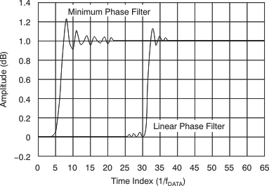
ADS1283 ai_fir_step_bas418.gifFigure 41. FIR Step Response