ZHCSK66C January 2014 – August 2019 ADS1283
PRODUCTION DATA.
- 1 特性
- 2 应用
- 3 说明
- 4 修订历史记录
- 5 Pin Configuration and Functions
- 6 Specifications
- 7 Parameter Measurement Information
-
8 Detailed Description
- 8.1 Overview
- 8.2 Functional Block Diagram
- 8.3 Feature Description
- 8.4
Device Functional Modes
- 8.4.1 Synchronization (SYNC PIN and SYNC Command)
- 8.4.2 Reset (RESET Pin and Reset Command)
- 8.4.3 Power-Down (PWDN Pin and STANDBY Command)
- 8.4.4 Power-On Sequence
- 8.4.5 DVDD Power Supply
- 8.4.6 Serial Interface
- 8.4.7 Data Format
- 8.4.8 Reading Data
- 8.4.9 One-Shot Operation
- 8.4.10 Offset and Full-Scale Calibration Registers
- 8.4.11 Calibration Commands (OFSCAL and GANCAL)
- 8.4.12 User Calibration
- 8.5
Programming
- 8.5.1
Commands
- 8.5.1.1 SDATAC Requirements
- 8.5.1.2 WAKEUP: Wake-Up From Standby Mode
- 8.5.1.3 STANDBY: Standby Mode
- 8.5.1.4 SYNC: Synchronize the Analog-to-Digital Conversion
- 8.5.1.5 RESET: Reset the Device
- 8.5.1.6 RDATAC: Read Data Continuous
- 8.5.1.7 SDATAC: Stop Read Data Continuous
- 8.5.1.8 RDATA: Read Data by Command
- 8.5.1.9 RREG: Read Register Data
- 8.5.1.10 WREG: Write to Register
- 8.5.1.11 OFSCAL: Offset Calibration
- 8.5.1.12 GANCAL: Gain Calibration
- 8.5.1
Commands
- 8.6
Register Maps
- 8.6.1
Register Descriptions
- 8.6.1.1 ID_CFG: ID_Configuration Register (address = 00h) [reset =x0h]
- 8.6.1.2 CONFIG0: Configuration Register 0 (address = 01h) [reset = 52h]
- 8.6.1.3 CONFIG1: Configuration Register 1 (address = 02h) [reset = 08h]
- 8.6.1.4 HPF0 and HPF1 Registers
- 8.6.1.5 OFC0, OFC1, OFC2 Registers
- 8.6.1.6 FSC0, FSC1, FSC2 Registers
- 8.6.1
Register Descriptions
- 9 Application and Implementation
- 10器件和文档支持
- 11机械、封装和可订购信息
8.4.1.2 Continuous-Sync Mode
In continuous-sync mode, either a single synchronization pulse or a continuous clock may be applied. When a single synchronization pulse is applied (rising edge), the device resynchronizes as it does in pulse-sync mode. ADC resynchronization occurs only under the condition that the time from the previous rising edge of SYNC is not a multiple of the conversion period. When resynchronization occurs in continuous-sync mode, DRDY continues to toggle unaffected, and the DOUT output is held low until data are ready (63 DRDY periods later). At the 63rd reading, conversion data are valid (when the conversion data are non-zero), as shown in Figure 45.
When a continuous clock is applied to the SYNC pin, the period must be an integral multiple of the output data rate or the device resynchronizes. Note that synchronization results in the restarting of the digital filter and an interruption of 63 readings (as shown in Table 12).
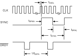
If a SYNC clock is applied to the ADC, the device resynchronizes only under the condition tSYNC ≠ N / fDATA, where N = 1, 2, 3, and so on. DRDY continues to output, but DOUT is held low until the new data are ready. If a SYNC clock is applied and the clock period matches an integral multiple of the output data rate, the device freely runs without resynchronization. Note that the phase of the applied clock and output data rate (DRDY) are not aligned because of the initial delay of DRDY after the SYNC clock is first applied. Figure 46 shows the timing for continuous-sync mode.
Apply a SYNC clock input after the continuous-sync mode is set. The first rising edge of SYNC then causes a synchronization. Note that subsequent writes to any ADC register results in resynchronization at the time of the register write operation. The resynchronization leads to loss of the SYNC-pin controlled synchronization performed previously. Send the STANDBY command followed by the WAKEUP command to reestablish the SYNC-pin synchronization. Resynchronization to the SYNC pin occurs as long as the time between the STANDBY and WAKEUP commands is not a multiple integer of the conversion period by at least one clock cycle.
