SWRA726 March 2022 CC1120 , CC1121 , CC1201 , CC1310 , CC1311P3 , CC1311R3 , CC1312PSIP , CC1312R , CC1312R7 , CC1314R10 , CC1350 , CC1352P , CC1352R , CC1354P10 , CC1354R10 , CC2340R5-Q1 , CC2640R2L , CC2651R3 , CC2652P , CC2652P7 , CC2652R , CC2652R7 , CC2652RB , CC2652RSIP , CC3130 , CC3135MOD , CC3230S , CC3235MODAS , CC3235MODASF , CC3235MODSF , CC3235S , WL1801MOD , WL1805MOD , WL1807MOD , WL1831 , WL1831MOD , WL1835MOD , WL1837MOD
- Trademarks
- 1Introduction
- 2Antenna Standing Wave Ratio (SWR) Measurement
- 3Evaluation Board Matching Components Location
- 4Volpert-Smith Chart
- 5868-MHz PCB Helix Antenna Measurement and Matching
- 62.4-GHz PCB Compact Antenna Measurement and Matching
- 7 2.4-GHz PCB Inverted-F Antenna Measurement and Matching
- 8Fast in-circuit or in-device Antenna Verification
- 9Conclusion
7 2.4-GHz PCB Inverted-F Antenna Measurement and Matching
A PCB inverted-F antenna is popular for Bluetooth®, Bluetooth® Low Energy, and ZigBee™ devices. It also can be used for Wi-Fi™ applications. Users can find the antenna's detailed description in the Application report DN007
The board was prepared for the tests and VNA calibration was done including matching network traces (refer to the Section 4.2).
 Figure 7-1 PCB Inverted-F Antenna
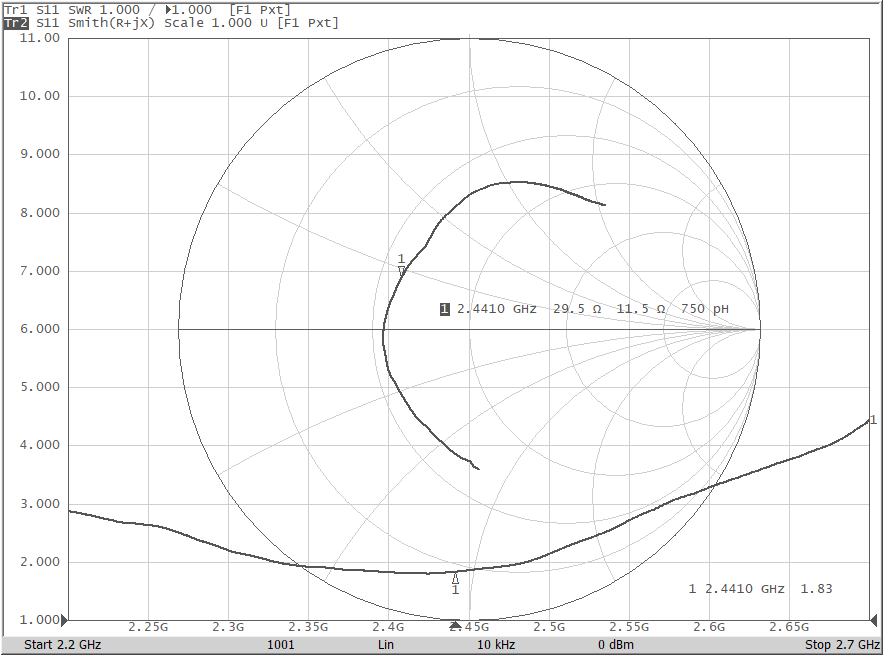
The impedance and SWR of unmatched antenna are shown in Figure 7-2. Markers are showing low, mid, and high operation frequencies for Bluetooth Low Energy and ZigBee applications. At 2.4410 GHz, the impedance is 29.5 + j11.5 Ohm and SWR value is 1.83:1.
 Figure 7-2 Measured Impedance of
Unmatched PCB Inverted-F Antenna at 2.4410 GHz
Figure 7-2 Measured Impedance of
Unmatched PCB Inverted-F Antenna at 2.4410 GHzFigure 4-4 shows that the network 4-4C and 4-4D can move the impedance to the center of the chart.
Online Smith chart calculators for the frequency at 2441 MHz and given impedance of 29.5 + j11.5 Ohm for network 4-4C gave values of 0.9 nH plus 1.1 pF. For small value capacitances (≤ 2 pF) usually recommended to pull back the ground plane a little on the top layer (not to affect the final capacitance and to use tight tolerances).
The network 4-4D with components values of 1.8 pF plus 3.9 nH was used. For matching job next steps were made:
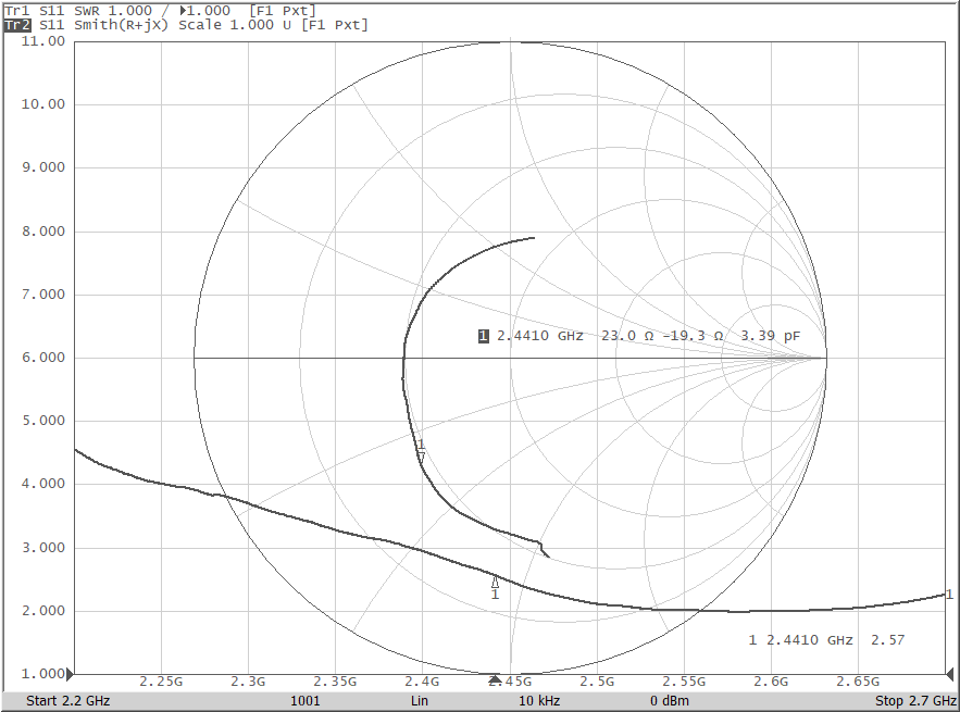
- The only capacitor of 1.8 pF was installed for checking how far the marker moves
(Figure 7-3).
 Figure 7-3 Measured Impedance
with only 1.8 pF Capacitor Installed
 - Installed inductor of 3.9 nH (1.8 pF and 3.9 nH)
- Adjusted inductor’s value to 4.3 nH (1.8 pF and 4.3 nH)
- Adjusted capacitor’s value to 2.0 pF (2.0 pF and 4.3 nH)
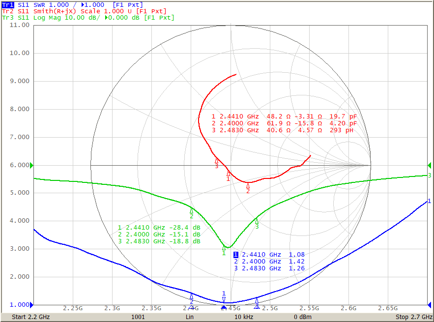
Figure 7-4 shows a final matched impedance with corresponded SWR and S11 levels. SWR value improved from 1:1.83 down to 1:1.08.
 Figure 7-4 Measured Impedance, SWR, and
S11 for Network 4-4D (with 2.0 pF and 4.3 nH)
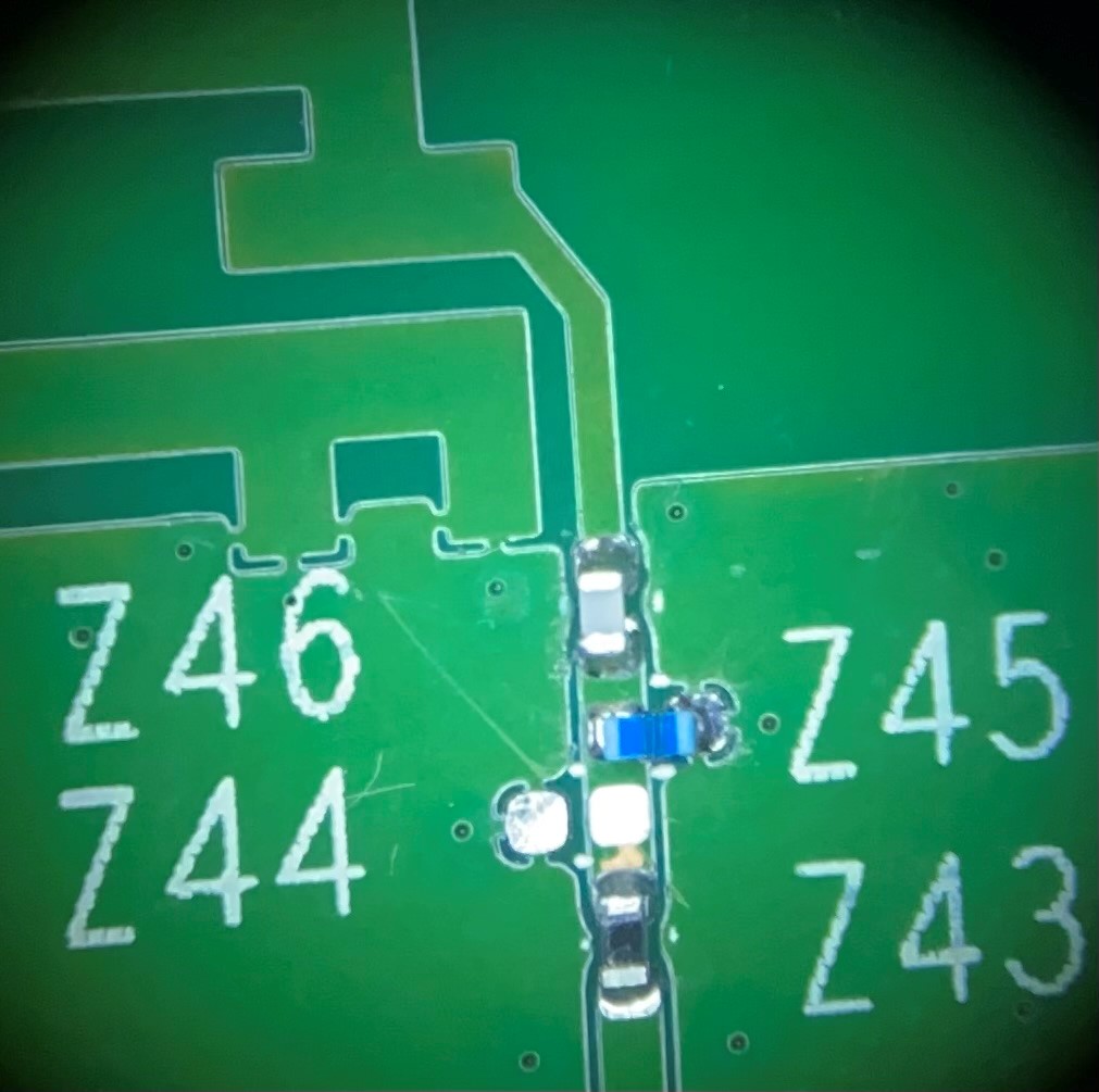
 Figure 7-5 Board with Final Matching
Components Installed