SSZT750 april 2018 CSD16401Q5 , CSD16415Q5 , CSD16556Q5B , CSD17556Q5B , CSD17559Q5 , CSD17573Q5B , CSD17575Q3 , CSD17576Q5B , CSD18531Q5A , CSD18532NQ5B , CSD18535KTT , CSD18536KTT , CSD18540Q5B , CSD19502Q5B , CSD19505KTT , CSD19506KTT , CSD19531Q5A , CSD19532KTT , CSD19532Q5B , CSD19535KTT , CSD19536KTT
Over the course of this series of blogs, I have covered a number of different FET applications, from motor control to power supply. Alas, I have arrived at the final topic – selecting a MOSFET for hot swap.
When a power supply is abruptly disconnected from its load, large current swings across the circuit’s parasitic inductive elements can generate dramatic voltage spikes that can be detrimental to the electrical components on the circuit. Similar to a battery protection application, here the MOSFET acts to insulate input power supply from the rest of the circuitry. In this case however, the FET is not meant to immediately sever the connection between input and output, but rather limit the severity of those destructive current surges. This is accomplished via a controller regulating the gate-to-source bias on a MOSFET placed in between an input power supply (VIN) and the output voltage (VOUT) forcing the MOSFET to operate in a saturation mode, and thus impeding the amount of current that can pass through (see Figure 1).
 Figure 1 Simplified Hot Swap
Circuit
Figure 1 Simplified Hot Swap
CircuitBefore anything else, your first consideration for this FET should be selecting an appropriate breakdown voltage, which is generally 1.5 to 2x the maximum input voltage. For instance, 12V systems tend to implement 25V or 30V FETs, and 48V systems tend to implement 100V or in some cases 150V FETS. The next consideration should be the MOSFET’s safe operating area (SOA) – a curve provided in the datasheet that is especially useful for indicating how susceptible a MOSFET is turn thermal runaway during short power surges not unlike those it must absorb in hot-swap applications. I wrote a post last year about how we at TI go about measuring and then generating the SOA of a MOSFET as it appears on the device’s datasheet. If you haven’t read that, you may want to consider giving it a skim, because for this application, the SOA is the most crucial criteria for making an appropriate selection.
The critical question for you, the designer, to ask is what is the maximum current surge that the FET might see (or be expected to limit to the output) and how long will this surge last. Once you know this, it is relatively simple to look up the corresponding current and voltage differential on the SOA figure in the device datasheet.
For instance, if your design has an input of 48V and you want to limit the current to the output to no more than 2A for 8ms, you could refer to the CSD19532KTT, CSD19535KTT and CSD19536KTT SOAs’ 10ms curves (Figure 2) and deduce that the latter two devices might work, whereas the CSD19532KTT would be insufficient. But since the CSD19535KTT is good enough with some margin, the performance of the more costly CSD19536KTT may be overkill for this application.
 Figure 2 The SOA of Three Different
100V D2PAK MOSFETs
Figure 2 The SOA of Three Different
100V D2PAK MOSFETsIn the example above, I assumed an ambient temperature of 25˚C, the same condition at which the SOA was measured at on the datasheet. But if the end application could be exposed to a much hotter environment, you must derate the SOA in proportion to how close the higher ambient temperature is to the FET’s maximum junction temperature. Let’s say for instance that the max ambient temperature of the end system is 70˚C; you would derate the curves of the SOA using Equation 1:
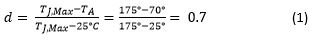
In this case, the CSD19535KTT’s 10ms, 48V capability would decrease from ~2.5A to ~1.8A. You would then deduce that particular FET would probably no longer be capable enough for this application and instead, select the CSD19536KTT.
It’s worth noting this method of derating assumes that the MOSFET will fail at exactly the max junction temperature, which is generally not the case. Say the failure points measured in the SOA testing actually occur at 200˚C or some other arbitrary higher value; the calculated derating will be closer to unity. That is to say, this derating methodology errs on the conservative side.
The SOA will also dictate the type of MOSFET package you select. D2PAK packages can house large silicon die, so they are very popular for higher-power applications. Smaller 5mm-by-6mm and 3.3mm-by-3.3mm quad flat no-lead (QFN) packages are preferable for lower-power applications. For current surges less than 5 – 10A, the FET is most often integrated with the controller.
A few final caveats:
- While I was speaking specifically to hot-swap applications here, you could apply the same SOA selection process to any situation where the FET operates in the saturation region. You could even use the same method for selecting a FET for OR-ing applications, power over Ethernet (PoE), or even slow switching applications like motor control, where there is going to be substantial high VDS and IDS overlap during MOSFET turn off.
- Hot swap is an application that tends to use surface-mount FETs as opposed to through-hole FETs (like TO-220s or I-PAK packages). The reason is that the heating that takes place for short pulse durations and thermal runaway events are very localized. In other words, the capacitive thermal impedance elements from the silicon junction to case prevent heat from dissipating into a board or heat sink fast enough to cool the junction. Junction-to-case thermal impedance (RθJC), a function of die size, is important, but junction-to-ambient thermal impedance (RθJA), a function of package, board and system thermal environment, is much less so. For that same reason, it is pretty rare to see heat sinks used for these applications.
- Designers often assume that the lowest-resistance MOSFET in a catalog will have the most capable SOA. There is some logic to this – lower resistance within the same silicon generation is usually indicative of a larger silicon die inside the package, which does yield greater SOA capability and lower junction-to-case thermal impedance. However, as silicon generations improve in resistance per unit area (RSP), they tend to increase in cell density. The denser the cell structure inside the silicon die, the more susceptible the die tends to be to thermal runaway. That is why older-generation FETs with much higher resistance sometimes also have much better SOA performance. The takeaway is that it always pays to investigate and compare the SOA.
- I would be remiss if I did not remind you (as I did in my blog post last year) not all datasheet SOAs are created equal, and you should not take all vendors’ SOAs at face value. Although TI certainly stands by the SOAs in its datasheets, it’s always best to have real data when possible.
TI has a number of hot swap controllers that you can learn more about here. For reference, Table 1-Table 3 at the end of this post highlight some devices we commonly recommend for hot swap, that provide some easy look up values for SOA capability.
That brings me to the conclusion of this MOSFET selection blog series. Thank you for reading, and I hope you learned something in the process. If you have any questions about this or any other post, feel free to post a comment below, or ask a question in TI’s E2E™ Community forum here.
| MOSFET | VDS (V) | Package | Typ RDS(ON) (mΩ) | SOA Current Rating (A) @ 14V VDS | |
|---|---|---|---|---|---|
| @ 10V VGS | 1ms | 10ms | |||
| CSD17575Q3 | 30 | SON3.3x3.3 | 1.9 | 4.5 | 2 |
| CSD17573Q5B | 30 | SON5x6 | 0.84 | 8 | 4.5 |
| CSD17576Q5B | 30 | SON5x6 | 1.7 | 8 | 4 |
| CSD16556Q5B | 25 | SON5x6 | 0.9 | 25 | 6 |
| CSD17559Q5 | 30 | SON5x6 | 0.95 | 30 | 14 |
| CSD17556Q5B | 30 | SON5x6 | 1.2 | 35 | 12 |
| CSD16401Q5 | 25 | SON5x6 | 1.3 | 100 | 15 |
| CSD16415Q5 | 25 | SON5x6 | 0.99 | 100 | 15 |
| MOSFET | VDS (V) | Package | Typ RDS(ON) (mΩ) | SOA Current Rating (A) @ 30V VDS | |||
|---|---|---|---|---|---|---|---|
| @ 10V VGS | 0.1ms | 1ms | 10ms | 100ms | |||
| CSD18531Q5A | 60 | SON5x6 | 3.5 | 28 | 9 | 3.8 | 0.9 |
| CSD19502Q5B | 80 | SON5x6 | 3.4 | 30 | 9 | 3.2 | 1 |
| CSD18532NQ5B | 60 | SON5x6 | 2.7 | 100 | 8.6 | 3 | 1.9 |
| CSD18540Q5B | 60 | SON5x6 | 1.8 | 105 | 13 | 4.9 | 2.2 |
| CSD19535KTT | 100 | D2PAK | 2.8 | 130 | 18 | 5.1 | 3 |
| CSD19505KTT | 80 | D2PAK | 2.6 | 200 | 18.5 | 5.3 | 3.4 |
| CSD18535KTT | 60 | D2PAK | 1.6 | 220 | 21 | 6.1 | 4.1 |
| CSD18536KTT | 60 | D2PAK | 1.3 | 220 | 31 | 9.5 | 5 |
| CSD19506KTT | 80 | D2PAK | 2.0 | 310 | 29 | 10 | 5.3 |
| CSD19536KTT | 100 | D2PAK | 2.0 | 400 | 34 | 10.5 | 5.4 |
| MOSFET | VDS (V) | Package | Typ RDS(ON) (mΩ) | SOA Current Rating (A) @ 60V VDS | |||
|---|---|---|---|---|---|---|---|
| @ 10V VGS | 0.1ms | 1ms | 10ms | 100ms | |||
| CSD19531Q5A | 100 | SON5x6 | 5.3 | 10 | 2.7 | 0.85 | 0.27 |
| CSD19532Q5B | 100 | SON5x6 | 4.0 | 9.5 | 3 | 1 | 0.33 |
| CSD19532KTT | 100 | D2PAK | 4.6 | 41 | 3.3 | 0.8 | 0.5 |
| CSD19535KTT | 100 | D2PAK | 2.8 | 46 | 6.1 | 1.9 | 1 |
| CSD19536KTT | 100 | D2PAK | 2.0 | 120 | 11 | 3.7 | 1.9 |