ZHCSMX7A August 2021 – December 2021 TPS92519-Q1
PRODUCTION DATA
- 1 特性
- 2 应用
- 3 说明
- 4 Revision History
- 5 Pin Configuration and Functions
- 6 Specifications
-
7 Detailed Description
- 7.1 Overview
- 7.2 Functional Block Diagram
- 7.3
Feature Description
- 7.3.1 Buck Converter Switching Operation
- 7.3.2 Switching Frequency and Adaptive On-Time Control
- 7.3.3 Minimum On-Time, Off-Time, and Inductor Ripple
- 7.3.4 Enable
- 7.3.5 LED Current Regulation and Error Amplifier
- 7.3.6 Start-up Sequence
- 7.3.7 Analog Dimming and Forced Continuous Conduction Mode
- 7.3.8 External PWM Dimming and Input Undervoltage Lockout (UVLO)
- 7.3.9 Shunt FET Dimming or Matrix Beam Application
- 7.3.10 Bias Supply
- 7.3.11 Bootstrap Supply
- 7.3.12 Faults and Diagnostics
- 7.3.13 Output Short Circuit Fault
- 7.3.14 Output Open Circuit Fault
- 7.3.15 Parallel Operation
- 7.4 Device Functional Modes
-
8 Application and Implementation
- 8.1
Application Information
- 8.1.1 Duty Cycle Consideration
- 8.1.2 Switching Frequency Selection
- 8.1.3 LED Current Set Point
- 8.1.4 Inductor Selection
- 8.1.5 Output Capacitor Selection
- 8.1.6 Input Capacitor Selection
- 8.1.7 Bootstrap Capacitor Selection
- 8.1.8 Compensation Capacitor Selection
- 8.1.9 Input Undervoltage Protection
- 8.1.10 CSN Protection Diode
- 8.2
Typical Application
- 8.2.1 Design Requirements
- 8.2.2
Detailed Design Procedure
- 8.2.2.1 Calculating Duty Cycle
- 8.2.2.2 Calculating Minimum On-Time and Off-Time
- 8.2.2.3 Minimum Switching Frequency
- 8.2.2.4 LED Current Set Point
- 8.2.2.5 Inductor Selection
- 8.2.2.6 Output Capacitor Selection
- 8.2.2.7 Bootstrap Capacitor Selection
- 8.2.2.8 Compensation Capacitor Selection
- 8.2.2.9 PWM Dimming and Input Voltage Protection
- 8.2.3 Application Curves
- 8.1
Application Information
- 9 Power Supply Recommendations
- 10Layout
- 11Device and Documentation Support
- 12Mechanical, Packaging, and Orderable Information
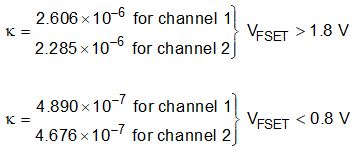
7.3.2 Switching Frequency and Adaptive On-Time Control
The TPS92519-Q1 uses an adaptive on-time control scheme and does not have a dedicated on-board oscillator. The one-shot timer is programmed by the voltage on FSET input. The on-time is calculated internally using Equation 1 and is inversely proportional to the measured input voltage, VIN, and proportional to the measured CSP voltage, VCSP.
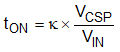
Constant, κ, is set by the FSET pin logic.
Given the duty ratio of the buck converter is VCSP / VIN, the switching period, TSW, remains nearly constant over all operating points. Use Equation 3 to calculate the switching period.
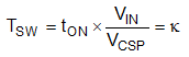
Use Equation 4 to calculate the switching frequency.
