ZHCSMX7A August 2021 – December 2021 TPS92519-Q1
PRODUCTION DATA
- 1 特性
- 2 应用
- 3 说明
- 4 Revision History
- 5 Pin Configuration and Functions
- 6 Specifications
-
7 Detailed Description
- 7.1 Overview
- 7.2 Functional Block Diagram
- 7.3
Feature Description
- 7.3.1 Buck Converter Switching Operation
- 7.3.2 Switching Frequency and Adaptive On-Time Control
- 7.3.3 Minimum On-Time, Off-Time, and Inductor Ripple
- 7.3.4 Enable
- 7.3.5 LED Current Regulation and Error Amplifier
- 7.3.6 Start-up Sequence
- 7.3.7 Analog Dimming and Forced Continuous Conduction Mode
- 7.3.8 External PWM Dimming and Input Undervoltage Lockout (UVLO)
- 7.3.9 Shunt FET Dimming or Matrix Beam Application
- 7.3.10 Bias Supply
- 7.3.11 Bootstrap Supply
- 7.3.12 Faults and Diagnostics
- 7.3.13 Output Short Circuit Fault
- 7.3.14 Output Open Circuit Fault
- 7.3.15 Parallel Operation
- 7.4 Device Functional Modes
-
8 Application and Implementation
- 8.1
Application Information
- 8.1.1 Duty Cycle Consideration
- 8.1.2 Switching Frequency Selection
- 8.1.3 LED Current Set Point
- 8.1.4 Inductor Selection
- 8.1.5 Output Capacitor Selection
- 8.1.6 Input Capacitor Selection
- 8.1.7 Bootstrap Capacitor Selection
- 8.1.8 Compensation Capacitor Selection
- 8.1.9 Input Undervoltage Protection
- 8.1.10 CSN Protection Diode
- 8.2
Typical Application
- 8.2.1 Design Requirements
- 8.2.2
Detailed Design Procedure
- 8.2.2.1 Calculating Duty Cycle
- 8.2.2.2 Calculating Minimum On-Time and Off-Time
- 8.2.2.3 Minimum Switching Frequency
- 8.2.2.4 LED Current Set Point
- 8.2.2.5 Inductor Selection
- 8.2.2.6 Output Capacitor Selection
- 8.2.2.7 Bootstrap Capacitor Selection
- 8.2.2.8 Compensation Capacitor Selection
- 8.2.2.9 PWM Dimming and Input Voltage Protection
- 8.2.3 Application Curves
- 8.1
Application Information
- 9 Power Supply Recommendations
- 10Layout
- 11Device and Documentation Support
- 12Mechanical, Packaging, and Orderable Information
8.1.7 Bootstrap Capacitor Selection
The bootstrap capacitor biases the high-side gate driver during the high-side FET on-time. The required capacitance depends on the PWM dimming frequency, PWMFREQ, and is sized to avoid boot undervoltage and fault during PWM dimming operation. Equation 19 calculates the bootstrap capacitance, CBST.
Equation 19. 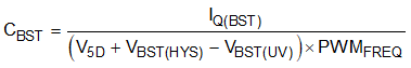
Table 8-2 summarizes the TI recommended bootstrap capacitor value for different PWM dimming frequencies.
Table 8-2 Bootstrap Capacitor Value
| PWM DIMMING FREQUENCY (Hz) | BOOTSTRAP CAPACITOR (µF) |
|---|---|
| 1507 | 0.1 |
| 1318 | 0.15 |
| 1055 | 0.22 |
| 879 | 0.22 |
| 659 | 0.33 |
| 439 | 0.47 |
| 215 | 1 |
| 108 | 2 |