ZHCSMX7A August 2021 – December 2021 TPS92519-Q1
PRODUCTION DATA
- 1 特性
- 2 应用
- 3 说明
- 4 Revision History
- 5 Pin Configuration and Functions
- 6 Specifications
-
7 Detailed Description
- 7.1 Overview
- 7.2 Functional Block Diagram
- 7.3
Feature Description
- 7.3.1 Buck Converter Switching Operation
- 7.3.2 Switching Frequency and Adaptive On-Time Control
- 7.3.3 Minimum On-Time, Off-Time, and Inductor Ripple
- 7.3.4 Enable
- 7.3.5 LED Current Regulation and Error Amplifier
- 7.3.6 Start-up Sequence
- 7.3.7 Analog Dimming and Forced Continuous Conduction Mode
- 7.3.8 External PWM Dimming and Input Undervoltage Lockout (UVLO)
- 7.3.9 Shunt FET Dimming or Matrix Beam Application
- 7.3.10 Bias Supply
- 7.3.11 Bootstrap Supply
- 7.3.12 Faults and Diagnostics
- 7.3.13 Output Short Circuit Fault
- 7.3.14 Output Open Circuit Fault
- 7.3.15 Parallel Operation
- 7.4 Device Functional Modes
-
8 Application and Implementation
- 8.1
Application Information
- 8.1.1 Duty Cycle Consideration
- 8.1.2 Switching Frequency Selection
- 8.1.3 LED Current Set Point
- 8.1.4 Inductor Selection
- 8.1.5 Output Capacitor Selection
- 8.1.6 Input Capacitor Selection
- 8.1.7 Bootstrap Capacitor Selection
- 8.1.8 Compensation Capacitor Selection
- 8.1.9 Input Undervoltage Protection
- 8.1.10 CSN Protection Diode
- 8.2
Typical Application
- 8.2.1 Design Requirements
- 8.2.2
Detailed Design Procedure
- 8.2.2.1 Calculating Duty Cycle
- 8.2.2.2 Calculating Minimum On-Time and Off-Time
- 8.2.2.3 Minimum Switching Frequency
- 8.2.2.4 LED Current Set Point
- 8.2.2.5 Inductor Selection
- 8.2.2.6 Output Capacitor Selection
- 8.2.2.7 Bootstrap Capacitor Selection
- 8.2.2.8 Compensation Capacitor Selection
- 8.2.2.9 PWM Dimming and Input Voltage Protection
- 8.2.3 Application Curves
- 8.1
Application Information
- 9 Power Supply Recommendations
- 10Layout
- 11Device and Documentation Support
- 12Mechanical, Packaging, and Orderable Information
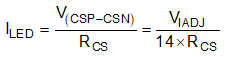
7.3.5 LED Current Regulation and Error Amplifier
The reference voltage, VIADJ, is internally scaled by a gain factor of 1/14 through a resistor network. An internal rail-to-rail error amplifier generates an error signal proportional to the difference between the scaled reference voltage (VIADJ / 14) and the inductor current measured by the differential voltage drop between CSP and CSN, V(CSP-CSN). This error drives the COMP pin voltage, VCOMP, and directly controls the valley threshold of the inductor current. Zero average DC error and closed-loop regulation is achieved by implementing an integral compensation network consisting of a capacitor connected from the output of the error amplifier to GND. As a good starting point, TI recommends a capacitor value between 1 nF and 10 nF between the COMP pin and GND. The choice of compensation network must ensure a minimum of 60° of phase margin and 10 dB of gain margin. The Application and Implementation section summarizes the detailed design procedure.
 Figure 7-2 Closed-loop LED Current
Regulation
Figure 7-2 Closed-loop LED Current
RegulationLED current is dependent on the current sense resistor, RCS. Use Equation 6 to calculate the LED current.
LED current accuracy is a function of the tolerance of the external sense resistor, RCS, and the variation in the sense threshold, V(CSP-CSN), caused by internal mismatch and temperature dependency of the analog components. The TPS92519-Q1 is capable of achieving LED current accuracy of ±4% at full scale over common-mode range and a junction temperature range of –40°C to 150°C.