ZHCSMX7A August 2021 – December 2021 TPS92519-Q1
PRODUCTION DATA
- 1 特性
- 2 应用
- 3 说明
- 4 Revision History
- 5 Pin Configuration and Functions
- 6 Specifications
-
7 Detailed Description
- 7.1 Overview
- 7.2 Functional Block Diagram
- 7.3
Feature Description
- 7.3.1 Buck Converter Switching Operation
- 7.3.2 Switching Frequency and Adaptive On-Time Control
- 7.3.3 Minimum On-Time, Off-Time, and Inductor Ripple
- 7.3.4 Enable
- 7.3.5 LED Current Regulation and Error Amplifier
- 7.3.6 Start-up Sequence
- 7.3.7 Analog Dimming and Forced Continuous Conduction Mode
- 7.3.8 External PWM Dimming and Input Undervoltage Lockout (UVLO)
- 7.3.9 Shunt FET Dimming or Matrix Beam Application
- 7.3.10 Bias Supply
- 7.3.11 Bootstrap Supply
- 7.3.12 Faults and Diagnostics
- 7.3.13 Output Short Circuit Fault
- 7.3.14 Output Open Circuit Fault
- 7.3.15 Parallel Operation
- 7.4 Device Functional Modes
-
8 Application and Implementation
- 8.1
Application Information
- 8.1.1 Duty Cycle Consideration
- 8.1.2 Switching Frequency Selection
- 8.1.3 LED Current Set Point
- 8.1.4 Inductor Selection
- 8.1.5 Output Capacitor Selection
- 8.1.6 Input Capacitor Selection
- 8.1.7 Bootstrap Capacitor Selection
- 8.1.8 Compensation Capacitor Selection
- 8.1.9 Input Undervoltage Protection
- 8.1.10 CSN Protection Diode
- 8.2
Typical Application
- 8.2.1 Design Requirements
- 8.2.2
Detailed Design Procedure
- 8.2.2.1 Calculating Duty Cycle
- 8.2.2.2 Calculating Minimum On-Time and Off-Time
- 8.2.2.3 Minimum Switching Frequency
- 8.2.2.4 LED Current Set Point
- 8.2.2.5 Inductor Selection
- 8.2.2.6 Output Capacitor Selection
- 8.2.2.7 Bootstrap Capacitor Selection
- 8.2.2.8 Compensation Capacitor Selection
- 8.2.2.9 PWM Dimming and Input Voltage Protection
- 8.2.3 Application Curves
- 8.1
Application Information
- 9 Power Supply Recommendations
- 10Layout
- 11Device and Documentation Support
- 12Mechanical, Packaging, and Orderable Information
7.3.6 Start-up Sequence
The start-up circuit allows the COMP pin voltage to gradually increase, thus reducing the LED current overshoot and current surges. The switching operation is initiated after the COMP pin voltage exceeds 2.45 V. A 450-mV hysteresis window allows the device to operate when COMP voltage is within the expected operating range of 2.2 V to 2.7 V. Switching is disabled on detection of low COMP voltage to avoid excessive negative inductor current.
 Figure 7-3 Soft-Start Sequence
The duration of soft start, tss, depends on the size of the compensation capacitor and the error amplifier source current, ICOMP(SRC).
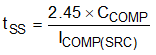
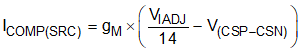
The source current, ICOMP(SRC) is a function of the transconductance, gM, of the error amplifier and error generated between the reference and the current sensed voltage.
With no current flowing through the LEDs, the soft start duration depends on the choice of compensation capacitor, CCOMP, and the reference voltage, VIADJ.
The open drain fault indicator, FLTx, is set low when the COMP voltage deviates from the nominal range and exceeds VCOMP(OV) threshold. This setting indicates a fault condition where the converter is operating in open-loop and the LED current is out of regulation. The corresponding channel can be disabled by setting IADJx input below 100 mV or controlling the UDIMx input.